RTL8181 데이터 시트보기 (PDF) - Realtek Semiconductor
부품명
상세내역
제조사
RTL8181 Datasheet PDF : 50 Pages
| |||
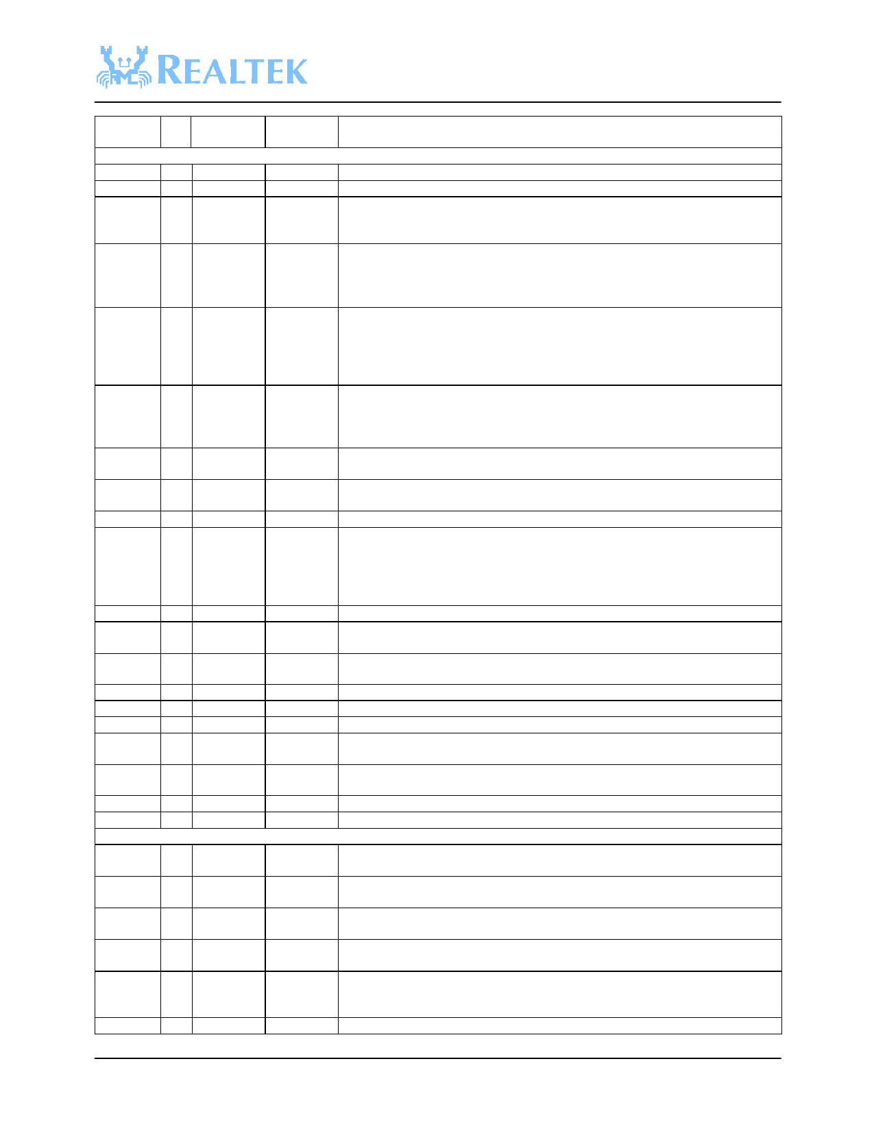
RTL8181
WLTXRX O 64
LED1B
RF Interface for Intersil
RIFSCK O 66
RIFSD O 67
RFLE O 68
IFLE/AGC O 70
SET
CALEN/ O 71
AGCRESE
T
LNA_HL O 73
ANTSELP O 75
ANTSELN O 76
TRSWP O 78
TRSWN O 79
VCOPDN/ O 81
PHITXI
PAPE O 82
PE1/PHIT O 84
XQ
PE2
O 85
RXIP
AI 110
RXIN AI 109
RXQP AI 106
RXQN AI
RSSI
AI 105
TXDET AI 102
VREFI AI 101
TXIP
AO 97
TXIN AO 96
TXQP AO 94
TXQN AO 93
TXAGC AO 91
RXAGC AO 90
RF Interface for RFMD
RIFSCK O 66
RIFSD O 67
RFLE O 68
IFLE/AGC X* 70
SET
CALEN/ X 71
AGCRESE
T
LNA_HL O 73
T18
WLAN Tx/Rx traffic indicator or JTAG CLK
R20
3-wire Bus Clock
P19
3-wire Bus Data
P18
3-wire Bus Enable
N18
IF_LE of the Intersil Chipset: PLL Synthesizer Serial Interface Latch Enable
Control. CMOS output.
P20
CAL_EN of the Intersil Chipset: CMOS output for activation of DC offset adjust
circuit. A rising edge activates the calibration cycle, which completes within a
programmable time and holds the calibration while this pin is held high. In
applications where the synthesizer is not used, this pin needs to be grounded.
M19
Drive to the RF AGC Stage Attenuator: CMOS digital.
M20
Antenna Select +: The antenna selects signal changes state as the receiver
switches from antenna to antenna during the acquisition process in the antenna
diversity mode. This is a complement for ANTSELN for differential drive of
ant enna switches.
L18
Antenna Select -: The antenna selects signal changes state as the receiver
switches from antenna to antenna during the acquisition process in the antenna
diversity mode. This is a complement for ANTSELP for differential drive of
antenna switches.
L19
Transmit/Receive Control
L20
K20
Output Pin as VCO VCC Power Enable/D isable.
K19
K18
J20
B19
B20
C18,C19
Transmit PA Power Enable
The combination of PE1 and PE2 are as follows:
00: Power Down State, PLL Registers in Save Mode, Inactive PLL, Active Serial
11: Receive State, Active PLL
10: Transmit State, Active PLL
01: Inactive Transmit and Receive States, Active PLL, Active Serial Interface
Output Pin as PE2: Refer to PE1 description.
Receive (Rx) In-phase Differential Analog Data
Receive (Rx) Quadrature Differential Analog Data
D17
D18
C20
E19,F18
Analog Input to the Receive Power A/D Converter for AGC Control
Input to the Transmit Power A/D Converter for Transmit AGC Control
Voltage Reference for ADC and DAC
Transmit (TX) In-phase Differential Analog Data
E20,F20 Trans mit (TX) Quadrature Differential Analog Data
F19
Analog Drive to the Transmit IF Power Control
G18
Analog Drive to the Receive IF AGC Control
R20
3-wire Bus Clock: The serial clock output, with resistive dividers on board to
allow programming from +5V levels.
P19
3-wire Bus Data: Serial data output, with resistive dividers on board to allow
programming from +5V levels.
P18
3-wire Bus Enable: Enable serial port output, with resistive dividers on board to
allow programming from +5V levels.
N18
Not used in the RFMD RF chipset.
P20
Not used in the RFMD RF chipset.
M19
RF2494 Gain Select: Digital output.
CONFIDENTIAL
7
v1.0
Share Link: 