RX2-433 데이터 시트보기 (PDF) - Radiometrix Ltd
부품명
상세내역
제조사
RX2-433 Datasheet PDF : 15 Pages
| |||
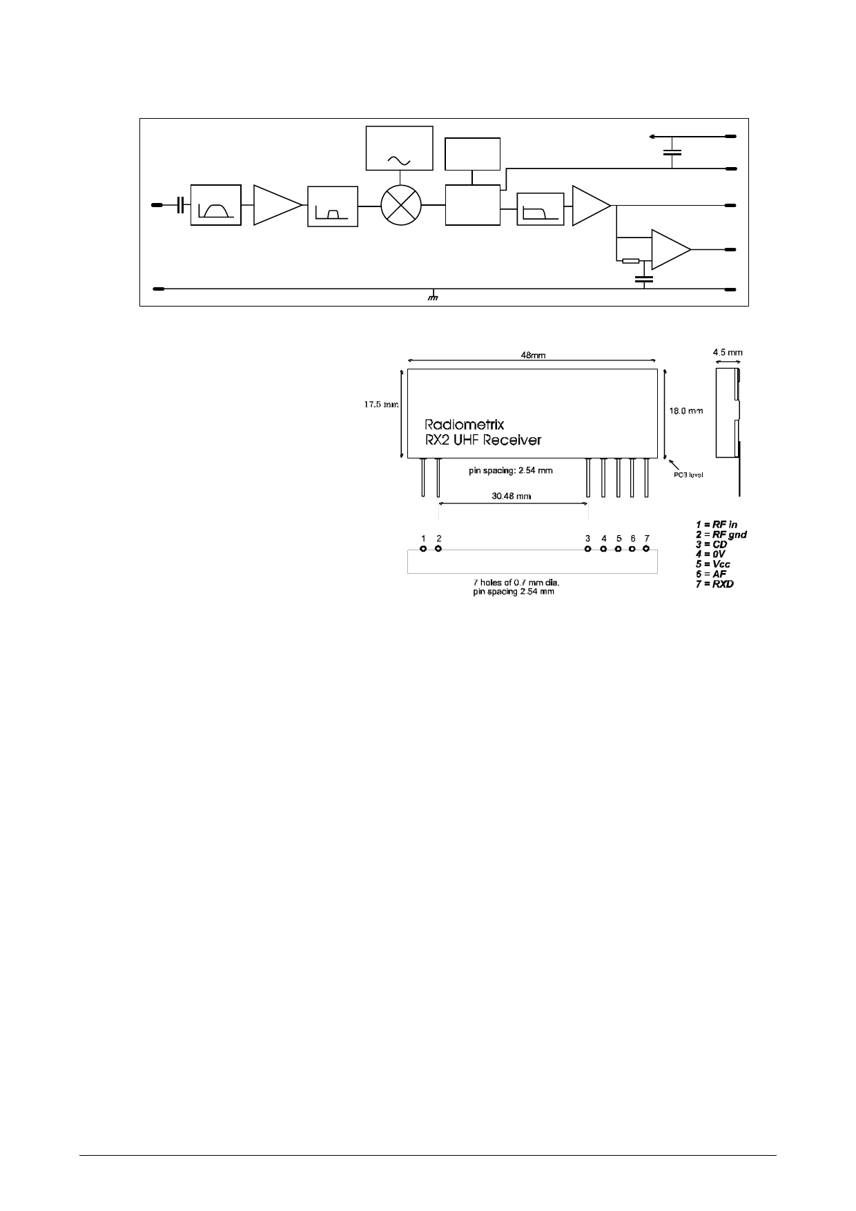
RX2 receiver:
418 MHz SAW-
controlled
1st Local oscillator
2nd local
oscillator
15.82 MHz
Vcc (5)
2µF
CD (3)
RF in (1) 433 MHz band
pass filter
pre -
amplifier
SAW band
pass filter
1st mixer
RF gnd (2)
2nd mixer
IF amlpifier
AF 91 kHz
demodulator
buffer
AF (6)
adaptive data slicer
+
Data out (7)
-
0 VOLT (4)
Pin description
Fig. 3: RX2 block diagram
RF in
(pin 1)
50Ω RF input from the antenna, it is
DC isolate internally. (see antenna
section for suggested antenna/feeds).
RF GND
(pin 2)
RF ground pin, internally connected to
the module screen and pin 4 (0V). This
pin should be connected to the RF
return path (e.g. coax braid, main
PCB ground plane etc.)
CD
(pin 3)
Fig. 4: physical dimensions
The Carrier Detect may be used to drive an external PNP transistor to obtain a logic level carrier detect
signal, see test circuit. If not required it should be connected to pin 5 (Vcc).
0 Volt
(pin 4)
Supply ground connection, connected to pin 1 and screen.
Vcc
(pin 5)
+ve supply pin. +3.0V to +6.0V @ <17mA . The supply must be clean < 2mVP-P ripple. A 10µF de-
coupling capacitor and 10Ω series resistor is recommended if a clean supply is not available.
AF
(pin 6)
This is a buffered and filtered analogue output from the FM demodulator. It has a standing DC bias of
1.2V and 400mV P-P base band signal. It is useful as a test point or to drive linear decoders. Load
impedance should be > 2kΩ and < 100pF.
RXD
(pin 7)
This digital output from the internal data slicer is a squared version of the signal on pin 6 (AF). It may
be used to drive external decoders. The data is true data, i.e. as fed to the transmitter. Load impedance
should be > 1kΩ and < 1nF
Radiometrix Ltd., TX2 & RX2 Data Sheet
page 3
Share Link: 