S3C7295 데이터 시트보기 (PDF) - Samsung
부품명
상세내역
제조사
S3C7295 Datasheet PDF : 31 Pages
| |||
PRODUCT OVERVIEW
S3C7295/P7295
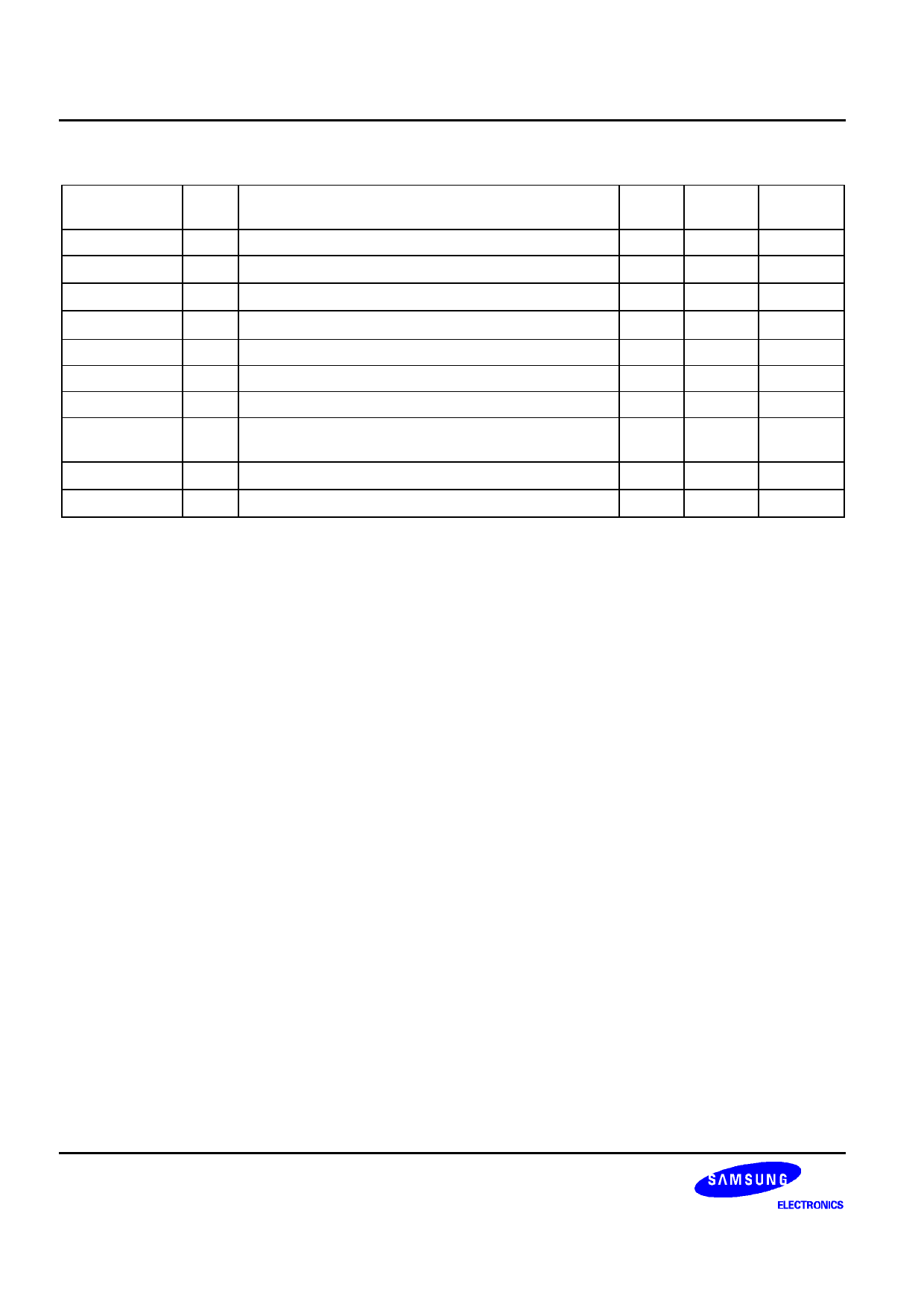
Table 1-1. S3C7295 Pin Descriptions (Continued)
Pin Name
K0–K3
VDD
VSS
RESET
CA, CB
VCL0
BIAS
Xin, Xout
XTin, XTout
TEST
Pin
Type
Description
I/O External interrupt (triggering edge is selectable)
– Power supply
– Ground
I Reset input (active low)
– Capacitor terminal for voltage doubling
– LCD power supply input
O Doubling voltage level output
– Crystal, ceramic or RC oscillator pins for system
clock
– Crystal oscillator pins for subsystem clock
I Test input (must be connected to VSS)
Circuit Number Share Pin
Type
E-1
11–8 P0.0–P0.3
–
12
–
–
13
–
B
19
–
–
20, 21
–
–
22
–
–
23
–
–
15, 14
–
–
17, 18
–
–
16
–
NOTE: Pull-up resistors for all I/O ports are automatically disabled if they are configured to output mode.
1-6
Share Link: 