S3C72N2 데이터 시트보기 (PDF) - Samsung
부품명
상세내역
제조사
S3C72N2 Datasheet PDF : 29 Pages
| |||
PRODUCT OVERVIEW
S3C72N2/C72N4/P72N4
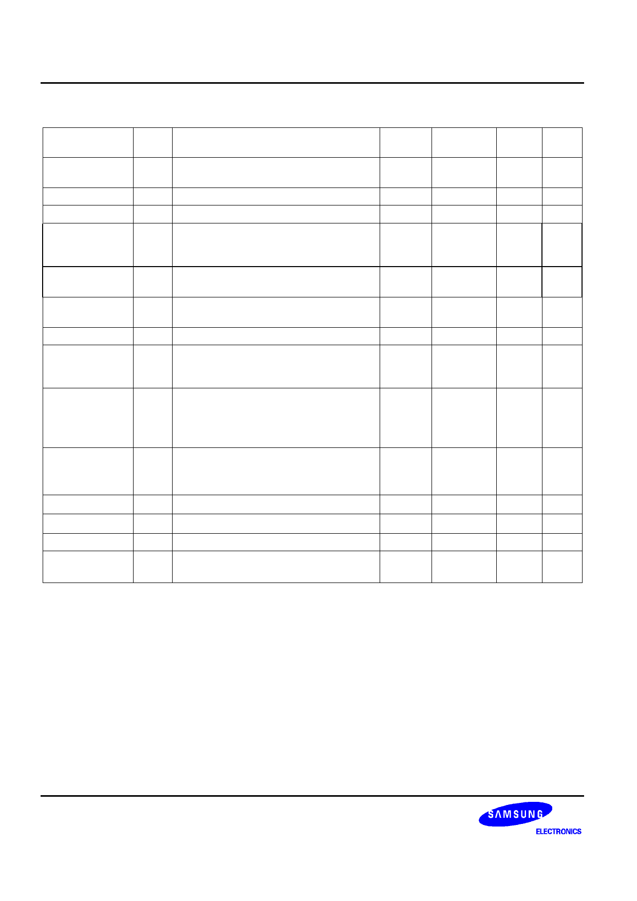
Table 1-1. S3C72N2/C72N4 Pin Descriptions (Continued)
Pin Name
LCDSY
TCL0
TCLO0
INT0
INT1
INT2
KS0–KS3
CLO
BUZ
XIN, XOUT
XTIN, XTOUT
VDD
VSS
RESET
TEST
Pin
Type
Description
Number
I/O LCD synchronization clock output for
26
LCD display expansion
I External clock input for timer/counter 0
20
I/O Timer/counter 0 clock output
21
I External interrupt. The triggering edge for 17
INT0 and INT1 is selectable. Only INT0 is 18
synchronized with the system clock.
I Quasi-interrupt with detection of rising
19
edge signals.
I/O Quasi-interrupt input with falling edge
detection.
29–32
I/O CPU clock output
23
I/O 2, 4, 8 or 16 kHz frequency output for
24
buzzer sound with 4.19 MHz main system
clock or 32.768 kHz subsystem clock.
– Crystal, ceramic or RC oscillator pins for 12,11
main system clock. (For external clock
input, use XIN and input XIN’s reverse
phase to XOUT)
– Crystal oscillator pins for subsystem
14,15
clock. (For external clock input, use XTIN
and input XTIN’s reverse phase to XTOUT)
– Main power supply
9
– Ground
10
– Reset signal
16
– Test signal input (must be connected to
13
VSS)
Share
Pin
P3.1
P1.3
P2.0
P1.0
P1.1
P1.2
P6.0–P6.3
P2.2
P2.3
–
–
–
–
–
–
Reset
Value
Input
Circuit
Type
D
Input A-4
Input D
Input A-4
Input A-4
Input D
Input D
Input D
–
–
–
–
–
–
–
–
Input B
–
–
NOTE: Pull-up resistors for all I/O ports automatically disabled if they are configured to output mode.
1-6
Share Link: 