SC1454 데이터 시트보기 (PDF) - Semtech Corporation
부품명
상세내역
제조사
SC1454 Datasheet PDF : 14 Pages
| |||
SC1454
POWER MANAGEMENT
Applications Information
Theory Of Operation
The SC1454 is intended for applications where very low
dropout voltage, low supply current and low output noise
are critical. Furthermore, the SC1454, by combining two
PulItNra Dlowesdcrroippotuiot n(UsLDO) regulators, along with enable
controls and output voltage adjustability for one output,
provides a very space efficient solution for multiple
supply requirements.
The SC1454 includes thermal shutdown circuitry to turn
off the device if TJ exceeds 150°C (typical), with the
device remaining off until TJ drops by 20°C (typical).
Reverse battery protection circuitry ensures that the
device cannot be damaged if the input supply is
accidentally reversed, limiting the reverse current to less
than 1.5mA.
Component Selection - General
The SC1454 contains two ULDOs, both of which are
supplied by one input supply, between IN and GND. Each
ULDO has its own active high enable pin (ENA/ENB).
Pulling this pin low causes that specific ULDO to enter a
very low power shutdown state.
The SC1454 contains an internal bandgap reference
which is fed into the inverting input of two error
amplifiers, one for each output. The output voltage of
each regulator is divided down internally using a resistor
divider and compared to the bandgap voltage. The error
amplifier drives the gate of a low RDS(ON) P-channel
MOSFET pass device.
Output A has both a fixed and adjustable output voltage
mode. Grounding the SETA pin (pulling it below the Sense/
Select threshold of 40mV) will connect the internal
resistor divider to the error amplifier resulting with the
internally preset output voltage. If SETA is pulled above
this threshold, then the Sense/Select switch will
connect the SETA pin to the error amplifier. Output A will
then be regulated such that the voltage at SETA will equal
VSETA, the SETA reference voltage (typically 1.250V).
A bypass pin (BYP) is provided to decouple the bandgap
reference to reduce output noise (on both outputs) and
also to improve power supply rejection.
Each regulator has its own current limit circuitry to
ensure that the output current will not damage the
device during output short, overload or start-up. The
current limit is guaranteed to be greater than 400mA to
allow fast charging of the output capacitor and high
initial currents for DSP initialization.
Output capacitor - Semtech recommends a minimum
capacitance of 1µF at the output with an equivalent
series resistance (ESR) of < 1Ω over temperature. While
the SC1454 has been designed to be used with ceramic
capacitors, it does not have to be used with ceramic
capacitors, allowing the designer a choice. Increasing the
bulk capacitance will further reduce output noise and
improve the overall transient response.
Input capacitor - Semtech recommends the use of a 1µF
ceramic capacitor at the input. This allows for the device
being some distance from any bulk capacitance on the
rail. Additionally, input droop due to load transients is
reduced, improving overall load transient response.
Bypass capacitor - Semtech recommends the use of a
10nF ceramic capacitor to bypass the bandgap
reference. Increasing this capacitor to 100nF will
further improve power supply rejection. Reducing this
capacitor below 1nF may result in output overshoot at
turn-on.
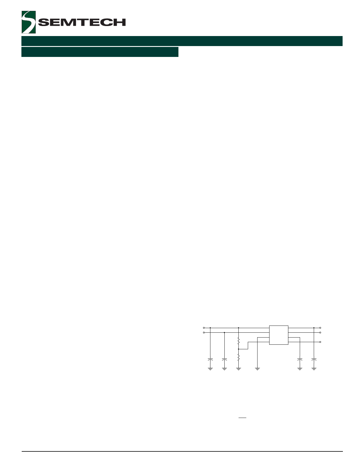
Component Selection - Externally Setting Output
OUTPUT A: 2.5V
OUTPUT B: 2.8V
R1
100k
U1 SC1454CIMS
1 OUTA
IN 8
2 OUTB
ENA 7
3 GND
BYP 6
4 SETA
ENB 5
VIN
ENABLE OUTPUT A
ENABLE OUTPUT B
R2
100k
C1
C2
1uF
1uF
C3
C4
10nF
1uF
Referring to the circuit above, the output voltage of
output A can be externally adjusted anywhere within the
range from 1.25V to (VIN(MAX) - VD(MAX)). The output voltage
will be in accordance with the following equation:
The SC1454 has a fast start-up circuit to speed up the
initial charging time of the bypass capacitor to enable
the output voltage to come up quicker.
VOUTA
=
1.250
•
1+
R1
R2
1% tolerance resistors are recommended. The values of
2005 Semtech Corp.
6
www.semtech.com
Share Link: 