MRFIC2002 데이터 시트보기 (PDF) - Motorola => Freescale
부품명
상세내역
제조사
MRFIC2002 Datasheet PDF : 6 Pages
| |||
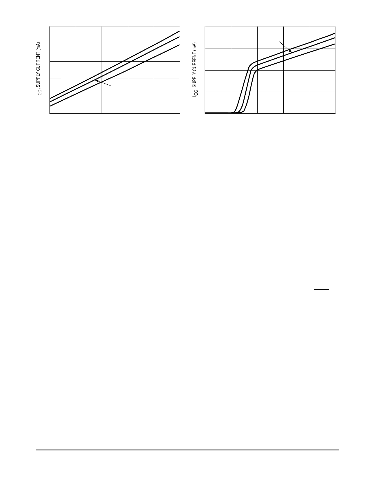
14
12
10
8
TA = +ā85°C
6
–ā35°C
25°C
4
3
3.4
3.8
4.2
4.6
VCC, SUPPLY VOLTAGE (V)
Figure 10. ICC versus VCC
8
25°C
TA = 85°C
6
–ā35°C
4
VCC = 3 V
2
0
5
0
1
2
3
4
5
VEN, ENABLE VOLTAGE (V)
Figure 11. ICC versus Enable Voltage
APPLICATIONS INFORMATION
DESIGN PHILOSOPHY
The MRFIC2002 was designed to have excellent LO and
spurious rejection. This is accomplished by using a double-
balanced configuration and using a symmetrical die layout.
To eliminate the need for external baluns or decoupling
elements, the unused LO and IF ports are decoupled inter-
nally. Only one of the RF outputs is used, eliminating the
need for an external balun on the RF port as well. Also, the
RF port is buffered to provide a 50 ohm output impedance.
External matching is required for the LO and IF ports.
To minimize current drain in various TDD/TDMA systems,
two methods of enabling/disabling the MRFIC2002 are pro-
vided: one that is TTL/CMOS compatible and one that is trig-
gered from a ramp, such as the one provided in the
MRFIC2004. The former method must be used if a ramp is
not available. The latter method is more desirable since the
MRFIC2002 can remain off during guard times and while in
idle mode.
THEORY OF OPERATION
Matching the LO port to 50 ohms can be done several
ways. The recommended approach is a series inductor as
close to the IC as possible. The inductor value is small
enough (~8 –15 nH depending on LO frequency) to be
printed on the board. A DC block is required and should not
be placed between the inductor and IC since this will prevent
the inductor from being placed close enough to the IC to pro-
vide a good match.
The IF port is approximately 500 ohms resistive in parallel
with 1.3 pF of capacitance. If 50 ohms is the desired IF port
impedance, a shunt capacitor followed by a series inductor
will provide the transformation. A DC block is required and
can be placed on either side of the matching network.
The RF port is nearly 50 ohms resistive in series with a
small amount of inductive reactance, which results in an
8 –11 dB return loss. However, a series 5.6 pF capacitor
placed as close to the IC as possible will typically provide
greater than a 15 dB return loss. The series capacitor also
serves as a DC block which is required.
Supply decoupling must be done as close to the IC as pos-
sible. A 1000 pF capacitor is recommended. An additional
100 pF capacitor and an RF choke are recommended to
keep the RF and LO signals off the supply line.
For systems that use a ramp, like the one provided in the
MRFIC2004, enabling/disabling can be done by applying the
ramp voltage to the VRAMP pin which trips the IC between
0.6 and 1.0 volts. The Enable pin must either be tied high or
to the inverse of the receiver enable control line, RXEN. An
inverter is provided in the MRFIC2004 to invert RXEN.
For systems that do not use a ramp, the VRAMP pin can
be left open circuited and enabling/disabling the MRFIC2002
can be done with its TTL/CMOS compatible Enable pin. The
trip point is between 1.0 and 2.0 volts.
EVALUATION BOARDS
Evaluation boards are available for RF Monolithic Inte-
grated Circuits by adding a “TF” suffix to the device type.
For a complete list of currently available boards and ones
in development for newly introduced product, please con-
tact your local Motorola Distributor or Sales Office.
MOTOROLA RF DEVICE DATA
MRFIC2002
5
Share Link: 