SG1524B 데이터 시트보기 (PDF) - Microsemi Corporation
부품명
상세내역
제조사
SG1524B Datasheet PDF : 5 Pages
| |||
SG1524B/SG2524B/SG3524B
ABSOLUTE MAXIMUM RATINGS (Note 1)
Input Voltage (+VIN) ..........................................................42V
Collector Voltage ............................................................. 60V
Logic Inputs ........................................................-.0..3V to 5.5V
Current Limit Sense Inputs ....................................-.0.3V to V
IN
Output Current (each transistor) ................................. 200mA
Reference Load Current ............................................... 50mA
Note 1. Values beyond which damage may occur.
Oscillator Charging Current ..............................................5mA
Operating Junction Temperature
Hermetic (J, L Packages) ...........................................1.50°C
Plastic (N, DW Packages) ..........................................1. 50°C
Storage Temperature Range ...........................-.65°C to 150°C
Lead Temperature (Soldering, 10 seconds) ...................300°C
RoHS Peak Package Solder Reflow Temp. (40 sec. max. exp.)...... 260°C(+0, -5)
THERMAL DATA
J Package:
Thermal Resistance-Junction to Case, θJC .................. 30°C/W
Thermal Resistance-Junction to Ambient, θJA ............... 80°C/W
N Package:
Thermal Resistance-Junction to Case, θJC .................. 40°C/W
Thermal Resistance-Junction to Ambient, θJA .............. 65°C/W
DW Package:
Thermal Resistance-Junction to Case, θJC ................... 40°C/W
Thermal Resistance-Junction to Ambient, θJA .............. 95°C/W
L Package:
Thermal Resistance-Junction to Case, θJC ................... 35°C/W
Thermal Resistance-Junction to Ambient, θJA ............ 120°C/W
Note A. Junction Temperature Calculation: TJ = TA + (PD x θJA).
Note B. The above numbers for θJC are maximums for the limiting
thermal resistance of the package in a standard mount-
ing configuration. The θJA numbers are meant to be
guidelines for the thermal performance of the device/pc-
board system. All of the above assume no ambient
airflow.
RECOMMENDED OPERATING CONDITIONS (Note 2)
Input Voltage (+V ) ................................................ 7V to 40V
IN
Collector Voltage .................................................... 0V to 60V
Error Amp Common Mode Range ....................... 2.3V to VREF
Current Limit Sense Common Mode Range ...... 0V to VIN-2.5V
Output Current (each transistor) .......................... 0 to 100mA
Reference Load Current ........................................ 0 to 20mA
Oscillator Charging Current ............................ 25µA to 1.8mA
Note 2: Range over which the device is functional.
Oscillator Frequency Range ........................ 100Hz to 400KHz
Oscillator Timing Resistor (RT) ......................... 2KΩ to 150KΩ
Oscillator Timing Capacitor (CT) ..........................1nF to 0.1µF
Operating Ambient Temperature Range
SG1524B .................................................... -55°C to 125°C
SG2524B ...................................................... -25°C to 85°C
SG3524B ......................................................... 0°C to 70°C
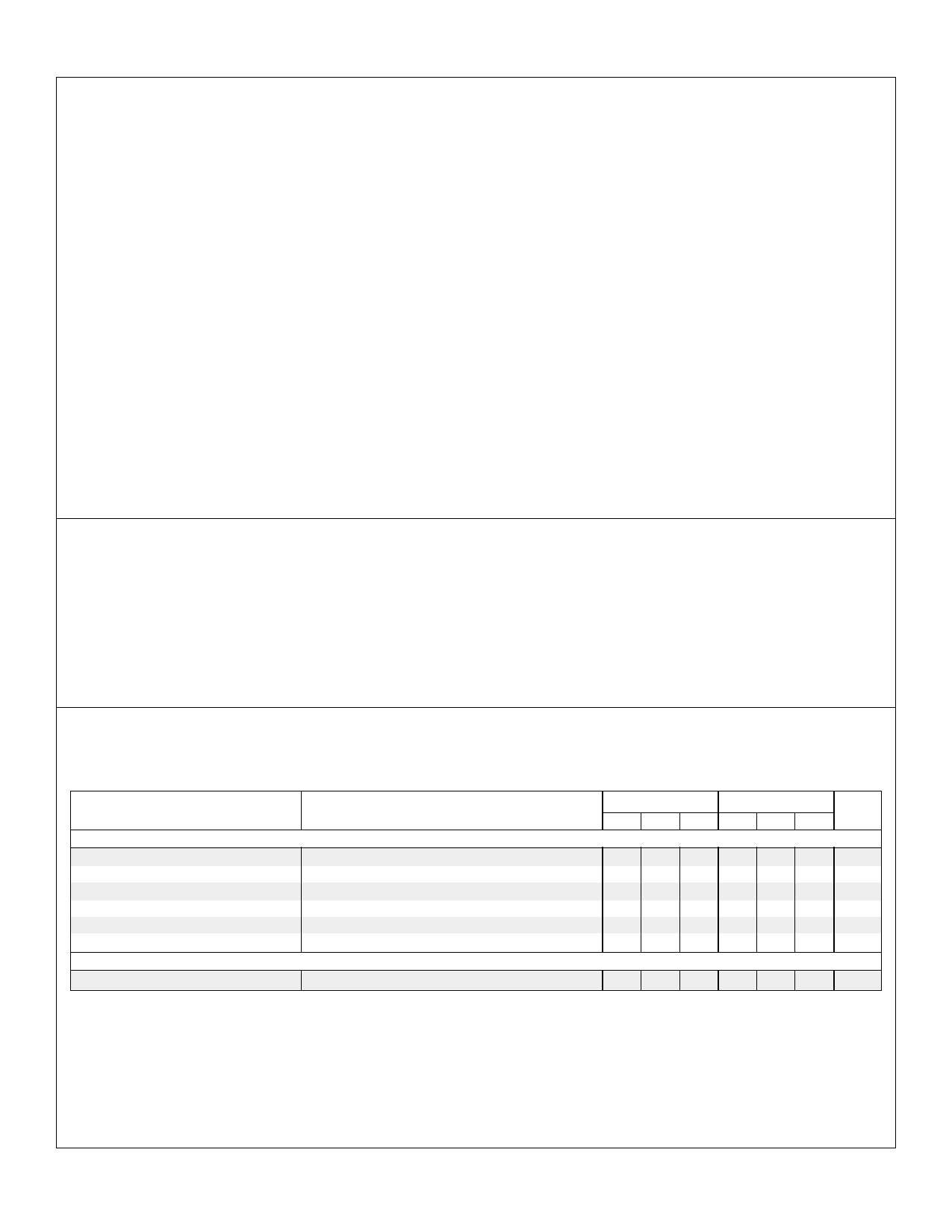
ELECTRICAL CHARACTERISTICS
(Unless otherwise specified, these specifications apply over the operating ambient temperatures for SG1524B with -55°C ≤ TA ≤ 125°C, SG2524B with -
25°C ≤ TA ≤ 85°C, SG3524B with 0°C ≤ TA ≤ 70°C, and +VIN = 20V. Low duty cycle pulse testing techniques are used which maintains junction and case
temperatures equal to the ambient temperature.)
Parameter
Reference Section (Note 3)
Output Voltage
Line Regulation
Load Regulation
Temperature Stability (Note 7)
Total Output Voltage Range
Short Circuit Current
Undervoltage Lockout Section
Threshold Voltage
Test Conditions
TJ = 25°C
VIN = 7V to 40V
IL = 0 to 20mA
Over Operating Temperature Range
Over Line, Load and Temperature
VREF = 0V
SG1524B/2524B
SG3524B
Units
Min. Typ. Max. Min. Typ. Max.
4.95 5.00 5.05 4.90 5.00 5.10 V
3 20
3 30 mV
5 30
5 50 mV
15 50
15 50 mV
4.90
5.10 4.80
5.20 V
25 50 120 25 50 120 mA
4.3 4.5 4.7 4.2 4.5 4.9 V
Note 3. IL = 0mA
Rev 1.3a
Copyright 2000
11861 Western Avenue ∞ Garden Grove, CA 92841
2
(714) 898-8121 ∞ FAX: (714) 893-2570
Share Link: 