SI5338G 데이터 시트보기 (PDF) - Silicon Laboratories
부품명
상세내역
제조사
SI5338G Datasheet PDF : 170 Pages
| |||
Si5338
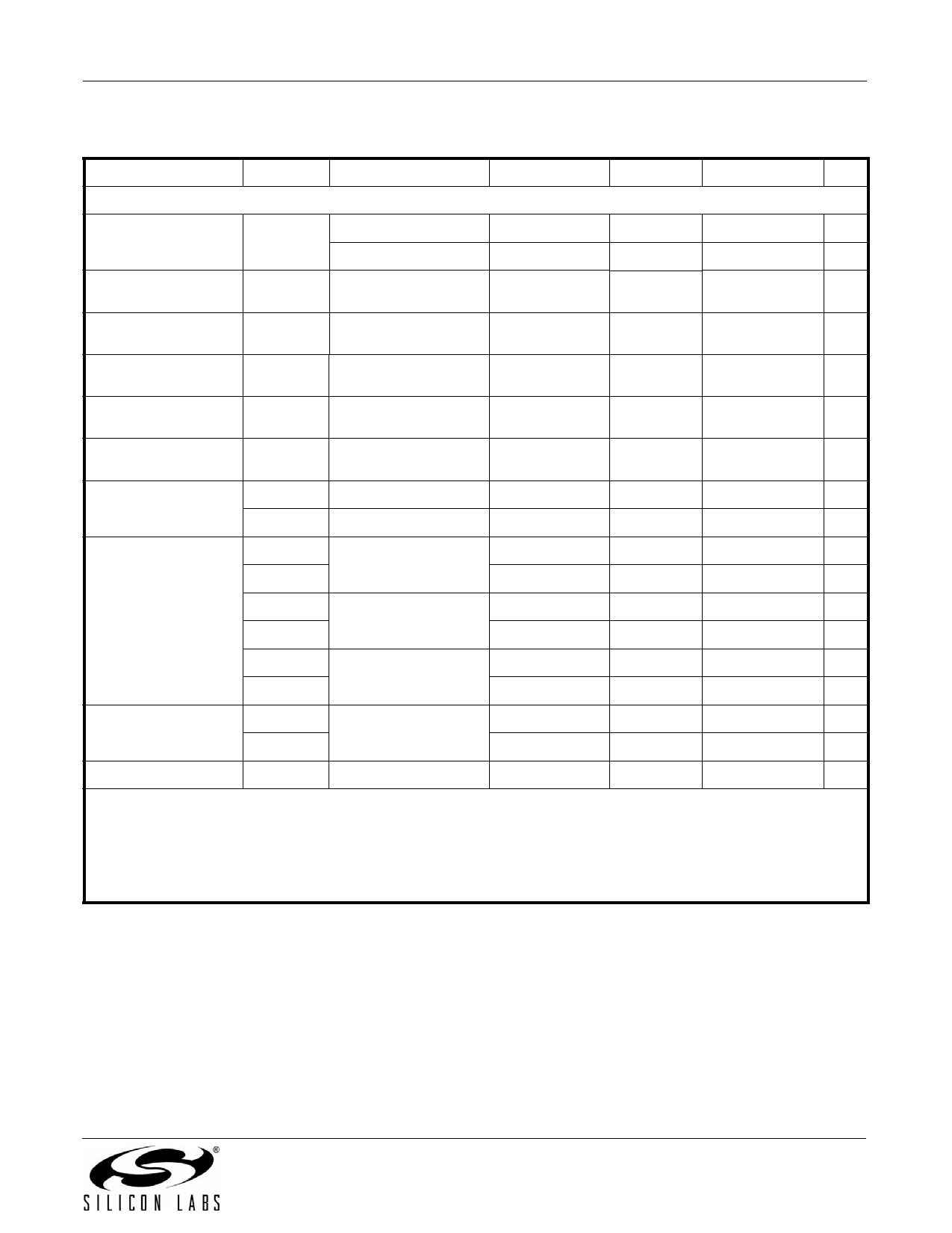
Table 6. Input and Output Clock Characteristics (Continued)
(VDD = 1.8 V –5% to +10%, 2.5 V ±10%, or 3.3 V ±10%, TA = –40 to 85 °C)
Parameter
Symbol
Test Condition
Min
Typ
Max
Units
Output Clocks (Single-Ended)
Frequency
fOUT
CMOS
SSTL, HSTL
0.16
—
0.16
—
200
MHz
350
MHz
CMOS 20%–80%
Rise/Fall Time
CMOS 20%–80%
Rise/Fall Time
CMOS Output Resis-
tance
SSTL Output
Resistance
HSTL Output
Resistance
CMOS Output Voltage5
SSTL Output Voltage
HSTL Output Voltage
Duty Cycle2
tR/tF
2 pF load
—
tR/tF
15 pF load
—
—
—
—
VOH
4 mA load
VDDO – 0.3
VOL
4 mA load
VOH
SSTL-3 VDDOx = 2.97 0.45xVDDO+0.41
VOL
to 3.63 V
—
VOH
SSTL-2 VDDOx = 2.25 0.5xVDDO+0.41
VOL
to 2.75 V
—
VOH
SSTL-18 VDDOx = 1.71 0.5xVDDO+0.34
VOL
to 1.98 V
—
VOH
0.5xVDDO+0.3
VDDO = 1.4 to 1.6 V
VOL
—
DC
45
0.45
—
50
50
50
—
—
—
—
—
—
—
—
—
—
—
0.85
ns
1.7
ns
—
—
—
V
0.3
V
—
V
0.45xVDDO–0.41 V
—
V
0.5xVDDO–0.41 V
V
0.5xVDDO–0.34 V
—
V
0.5xVDDO –0.3 V
55
%
Notes:
1. For best jitter performance, keep the input slew rate on pins 1,2,5,6 faster than 0.3 V/ns
2. Not in PLL bypass mode.
3. For best jitter performance, keep the input single ended slew rate on pins 3 or 4 faster than 1 V/ns
4. Only two unique frequencies above 350 MHz can be simultaneously output, Fvco/4 and Fvco/6.
5. Includes effect of internal series 22 resistor.
Rev. 0.6
9
Share Link: 