SIP11203DB 데이터 시트보기 (PDF) - Vishay Semiconductors
부품명
상세내역
제조사
SIP11203DB Datasheet PDF : 12 Pages
| |||
MULTILAYER PCB DESIGN FOR POWER
TRANSFORMER
Layer
1
2
3
4
5
6
7
8
Winding
P1
S1
P2
S2
P3
S3
P4
S4
No. of Turns
1
1
1
1
1
1
1
1
Table 1.
B1
B2
Vbias
L1
L2
L3
VO
L4
L5
L6
Figure 8. Power Inductor Structure
MULTILAYER PCB DESIGN FOR POWER
INDUCTOR
Layer
1
2
3
4
5
6
7
8
Winding
L1
L2
L3
B1
B2
L4
L5
L6
No. of Turns
1
1
1
5
5
1
1
1
Table 2.
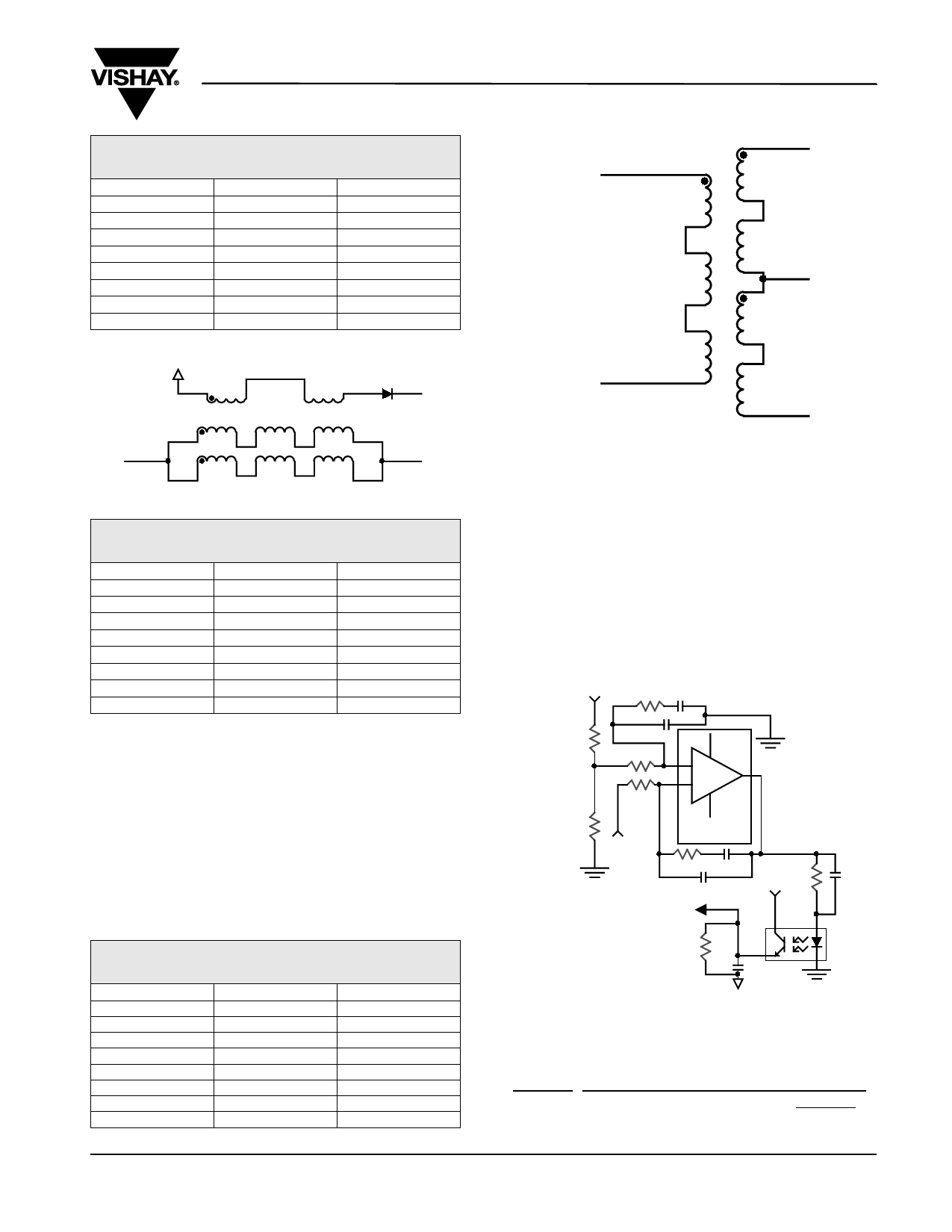
The pulse transformer structure is illustrated in Figure
9. The multilayer PCB layout is described in Table 3.
The primary magnetizing inductance is between 90 µH
and 130 µH, and the turn ratio is 8:6:6. The core is a
combination of two E8.8 cores in high permeability T38
material from EPCOS. These cores must be aligned
very carefully, and glued together while clamped, with
no glue being placed between the core legs, in order to
ensure the required magnetizing inductance. If the
magnetizing inductance is too low, the Si9122 will be
overloaded, and the circuit will not function.
MULTILAYER PCB DESIGN FOR PULSE
TRANSFORMER
Layer
1
2
3
4
5
6
7
8
Winding
Pa
Sa
Sb
Pb
Sc
Sd
Pc
-
No. of Turns
3
3
2
3
3
3
3
-
Table 3.
Document Number: 74254
S-60997–Rev. A, 12-Jun-06
SiP11203DB
Vishay Siliconix
Sa
Pa
Sb
Pb
Sc
Pc
Sd
Figure 9. Pulse Transformer Structure
Controller
The SiP11203 possesses a voltage reference and Op
Amp, which can be used to control the output voltage.
The reference voltage VREF is compared with the
scaled output voltage, and the compensated error volt-
age drives the opto-coupler diode U3-A. The current in
the opto-coupler transistor U3-B is converted to a volt-
age signal by R13 and this signal is applied to the EP
pin of the Si9122, where it is converted to a PWM out-
put.
The compensation structure is depicted in Figure 10.
Vo
R8 C25
R1
C29
R5
+
R6
-
R2//R37
Vref
SiP11203
R7
C1
R9
C4
C2
Vcc
EP
U3
R13
C7
Figure 10. Controller Compensation Structure
The equation describing the compensation circuitry is:
R13 CTR
R9
(1 + S R7C1)(1 + S R9C4)
( )( ) ( S R6 C1+ C2 1 + S R13 C7
1+
S R2
C1C2
C1 + C2
)
www.vishay.com
5
Share Link: 