SL6619 데이터 시트보기 (PDF) - Mitel Networks
부품명
상세내역
제조사
SL6619 Datasheet PDF : 21 Pages
| |||
Supersedes July 1996 version, DS3853 - 3.5
The SL6619 is an advanced Direct Conversion FSK Data
Receiver for operation up to 450 MHz. The device integrates all
functions to convert a binary FSK modulated RF signal into a
demodulated data stream.
Adjacent channel rejection is provided using tuneable gyrator
filters. RF and audio AGC functions assist operation when large
interfering signals are present and an automatic frequency control
(AFC) function is provided to extend centre frequency acceptance.
FEATURES
s Very Low Power Operation from Single Cell
s Superior Sensitivity
s Operation at 512, 1200 and 2400 Baud
s On Chip 1 Volt Regulator
s 1mm Height Miniature Package
s Automatic Frequency Control Function
s Programmable Post Detection Filter
s AGC Detection Circuitry
s Power Down Function
s Battery Strength Indicator
APPLICATIONS
s Pagers, including Credit Card, PCMCIA and
Watch Pagers
s Low Data Rate Receivers, e.g. Security Systems
ORDERING INFORMATION
SL6619/KG/TP1N 1mm TQFP device, baked and dry
packed, supplied in trays
SL6619/KG/TP1Q 1mm TQFP device, baked and dry
packed, supplied in tape and reel
SL6619
Direct Conversion FSK Data Receiver
Preliminary Information
DS3853 - 4.1 April 1998
IRF
GND
MIXIP A
MIX DEC
MIXIP B
REG CNT
VREG
TPI
32 31 30 29 28 27 26 25
1
24
2
23
3
22
4
5
SL6619
21
20
6
19
7
18
8
17
9 10 11 12 13 14 15 16
AFC1
BATT FLAG
VCC2
DATA OP
BEC
AFC OP
VREF
TPQ
TP32
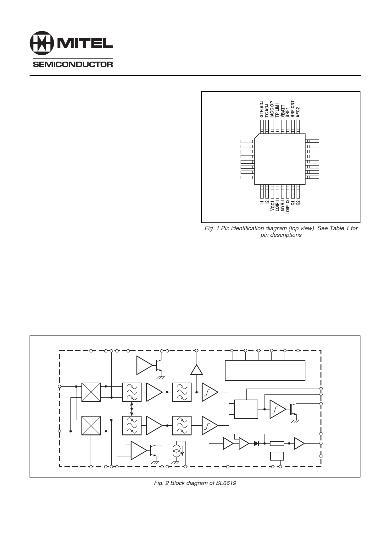
Fig. 1 Pin identification diagram (top view). See Table 1 for
pin descriptions
ABSOLUTE MAXIMUM RATINGS
Storage temperature
Operating temperature
Maximum voltage on any pin w.r.t. any
255°C to1150°C
210°C to155°C
14V
other pin, subject to the following conditions:
Current, pin 3 (MIXIP), pin 5 (MIXPB),
<5ma
pin 12 (LOIPI) and pin 14 (LOIPB)
Most negative voltage on any pin
20·5V w.r.t. gnd
12 9 10 13 7
68
29
−
1·0V +
4 20 11 22 2 18
MIX BEC VCC1 VCC2 GND VREF
DEC
3
MIXER
5
1·08V −
+
26
27
LIMITER
4f
21
DETECTOR
LIMITER
31
30
AFC
19
14 15 16 28
23 17
1
32
Fig. 2 Block diagram of SL6619
24 25
Share Link: 