SM802117 데이터 시트보기 (PDF) - Micrel
부품명
상세내역
제조사
SM802117 Datasheet PDF : 10 Pages
| |||
Micrel, Inc.
SM802117
Absolute Maximum Ratings(1)
Supply Voltage (VDD, VDDO1/2) ......................................+4.6V
Input Voltage (VIN). ............................. –0.50V to VDD + 0.5V
Lead Temperature (soldering, 20sec.)....................... 260°C
Case Temperature ..................................................... 115°C
Storage Temperature (Ts) .........................–65°C to +150°C
Operating Ratings(2)
Supply Voltage (VDD, VDDO1/2)............... +2.375V to +3.465V
Ambient Temperature (TA) .......................... –40°C to +85°C
Junction Thermal Resistance(3)
QFN (θJA)
Still-Air ......................................................... 50°C/W
QFN (ψJB)
Junction-to-Board .......................................30°C/W
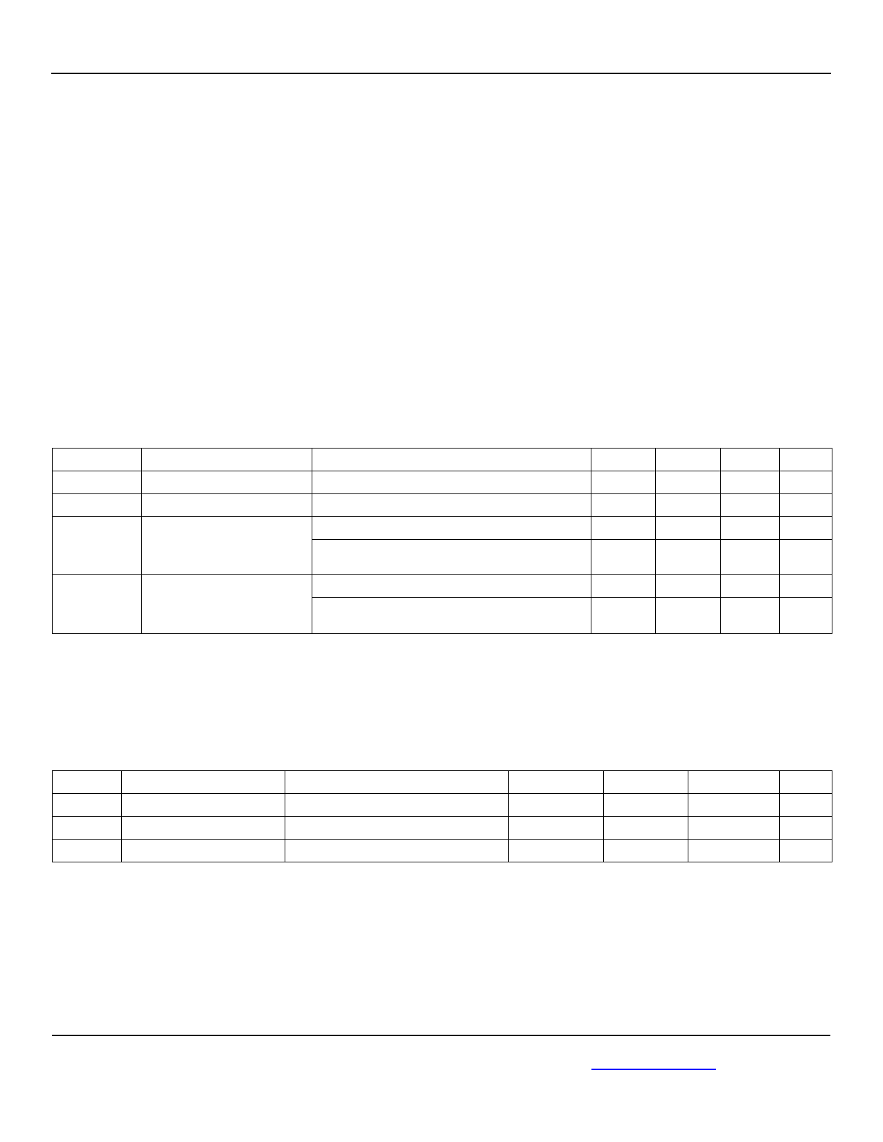
DC Electrical Characteristics(4)
VDD = VDDO1/2 = 3.3V ±5% or 2.5V ±5%
VDD = 3.3V ±5%, VDDO1/2 = 2.5V ±5%
TA = −40°C to +85°C.
Symbol
Parameter
VDD, VDDO1/2 2.5V Operating Voltage
VDD, VDDO1/2 3.3V Operating Voltage
IDD
REF_IN
Supply current VDD + VDDO
XTAL_SEL = 0
Outputs open
IDD
XTAL
Supply current VDD + VDDO
XTAL_SEL = 1
Outputs open
Condition
125MHz - 1 output
125MHz - 2 outputs
125MHz - 1 output
125MHz - 2 outputs
Min.
2.375
3.135
Typ.
2.5
3.3
97
114
87
104
Max.
2.625
3.465
125
148
113
135
Units
V
V
mA
mA
mA
mA
LVPECL OUTPUT DC Electrical Characteristics(4)
VDD = VDDO1/2 = 3.3V ±5% or 2.5V ±5%
VDD = 3.3V ±5%, VDDO1/2 = 2.5V ±5%
TA = −40°C to +85°C. RL = 50Ω to VDDO − 2V
Symbol Parameter
Condition
VOH
Output High Voltage
VOL
Output Low Voltage
VSWING
Output Voltage Swing
Min.
VDDO – 1.145
VDDO – 1.945
0.6
Typ.
VDDO – 0.97
VDDO – 1.77
0.8
Max.
VDDO – 0.845
VDDO – 1.645
1.0
Units
V
V
V
Note:
1. Permanent device damage may occur if absolute maximum ratings are exceeded. This is a stress rating only and functional operation is not implied
at conditions other than those detailed in the operational sections of this data sheet. Exposure to absolute maximum rating conditions for extended
periods may affect device reliability.
2. The data sheet limits are not guaranteed if the device is operated beyond the operating ratings.
3. Package thermal resistance assumes exposed pad is soldered (or equivalent) to the devices most negative potential on the PCB.
4. The circuit is designed to meet the AC and DC specifications shown in the above table(s) after thermal equilibrium has been established.
October 2011
4
M9999-101311-B
hbwhelp@micrel.com or (408) 955-1690
Share Link: 