SM802128 데이터 시트보기 (PDF) - Micrel
부품명
상세내역
제조사
SM802128 Datasheet PDF : 12 Pages
| |||
Micrel, Inc.
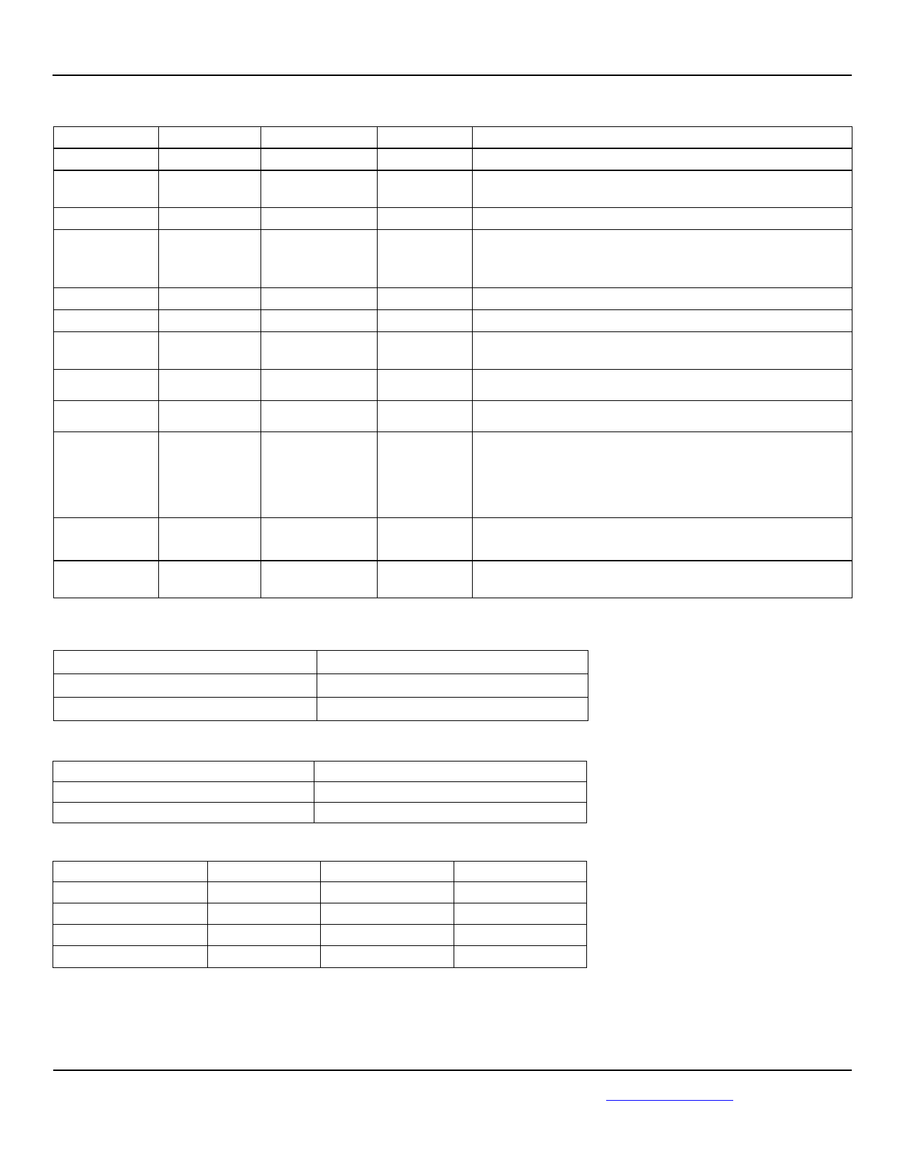
Pin Description (continued)
Pin Number
3, 6, 40
11, 20, 27, 30,
34
12, 13
21, 23
17
18
Pin Name
VSSO2
TEST
VDD
VSS
(Exposed
Pad)
REF_IN
XTAL_IN
Pin Type
PWR
PWR
PWR
I, (SE)
I, (SE)
19
XTAL_OUT
O, (SE)
15
OE1
I, (SE)
22
OE2
I, (SE)
9
PLL_BYPASS
I, (SE)
10
XTAL_SEL
14
FSEL
Truth Tables
OE1/2
0
1
I, (SE)
I, (SE)
SM802128
Pin Level
LVCMOS
Crystal
Crystal
LVCMOS
LVCMOS
LVCMOS
LVCMOS
LVCMOS
Pin Function
Power Supply Ground for the Outputs on Bank 2
Factory Test Pins. Do not connect anything to these pins.
Core Power Supply
Core Power Supply Ground. The exposed pad must be
connected to the VSS ground plane.
Reference Clock Input
Crystal Reference Input, no load caps needed (See Figure 5).
Crystal Reference Output, no load caps needed (See Figure
5).
Output Enable, Q1-Q4 disables to tri-state, 0 = Disabled, 1 =
Enabled, 45KΩ Pull-Up.
Output Enable, Q5-Q8 disables to tri-state, 0 = Disabled, 1 =
Enabled, 45KΩ Pull-Up.
PLL Bypass, Selects Output Source
0 = Normal PLL Operation
1 = Output from Input Reference Clock or Crystal
45KΩ Pull-Down
Selects PLL Input Reference Source
0 = REF_IN, 1 = XTAL, 45KΩ Pull-Up
Frequency Select, 1 = 156.25MHz, 0 = 312.5MHz,
45KΩ Pull-Up
Tri-state
LVPECL
FSEL
0
1
PLL_BYPASS/CSB
0
1
−
−
XTAL_SEL
−
−
0
1
Output Frequency (MHz)
312.5
156.25
−
−
REF_IN
XTAL
PLL
XTAL/REF_IN
−
−
January 2012
3
hbwhelp@micrel.com or (408) 955-1690
Share Link: 