SMK0465FJ 데이터 시트보기 (PDF) - Kodenshi Auk Co., LTD
부품명
상세내역
제조사
SMK0465FJ Datasheet PDF : 8 Pages
| |||
SMK0465FJ
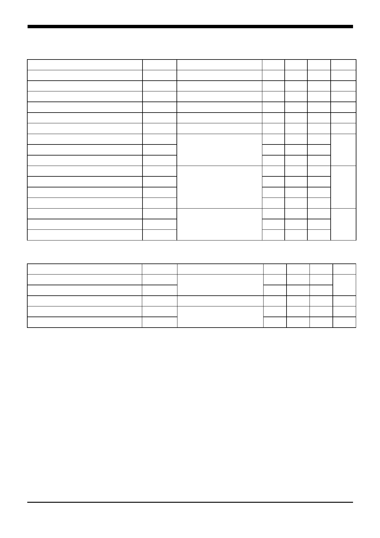
Electrical Characteristics (TC=25C unless otherwise noted)
Characteristic
Symbol
Test Condition
Drain-source breakdown voltage
Gate threshold voltage
Drain-source cut-off current
Gate leakage current
Drain-source on-resistance
④
Forward transfer conductance ④
Input capacitance
Output capacitance
Reverse transfer capacitance
BVDSS
VGS(th)
IDSS
IGSS
RDS(ON)
gfs
Ciss
Coss
Crss
ID=250A, VGS=0
ID=250A, VDS=VGS
VDS=650V, VGS=0V
VDS=0V, VGS=30V
VGS=10V, ID=2.0A
VDS=10V, ID=2.0A
VGS=0V, VDS=25V,
f=1MHz
Turn-on delay time
Rise time
Turn-off delay time
Fall time
Total gate charge
Gate-source charge
Gate-drain charge
td(on)
tr
td(off)
tf
Qg
Qgs
Qgd
VDD=300V, ID=4.0A
RG=25Ω
③④
VDS=520V, VGS=10V
ID=4.0A
③④
Min.
650
2.0
-
-
-
-
-
-
-
-
-
-
-
-
-
-
Typ.
-
-
-
-
2.4
4.0
703
54.6
5.6
10
42
38
46
11.2
3.9
2.5
Max.
-
4.0
1
100
3.0
-
878
68.2
7.0
-
-
-
-
14.0
-
-
Unit
V
V
uA
nA
S
pF
ns
nC
Source-Drain Diode Ratings and Characteristics (TC=25C unless otherwise noted)
Characteristic
Symbol
Test Condition
Min. Typ. Max.
Source current (DC)
Source current (Pulsed)
IS
Integral reverse diode
①
ISM
in the MOSFET
-
-
4
-
-
16
Forward voltage
④
VSD
VGS=0V, IS=4.0A
-
-
1.4
Reverse recovery time
Reverse recovery charge
trr
IS=4.0A, VGS=0V
Qrr
dIF/dt=100A/us
-
300
-
-
2.2
-
Unit
A
V
ns
uC
Note ;
① Repetitive rating : Pulse width limited by maximum junction temperature
② L=9.4mH, IAS=4.0A, VDD=50V, RG=25Ω, Starting TJ=25℃
③ Pulse Test : Pulse width≤300us, Duty cycle≤2%
④ Essentially independent of operating temperature
KSD-T0O065-000
2
Share Link: 