SMK0825 데이터 시트보기 (PDF) - Kodenshi Auk Co., LTD
부품명
상세내역
제조사
SMK0825 Datasheet PDF : 8 Pages
| |||
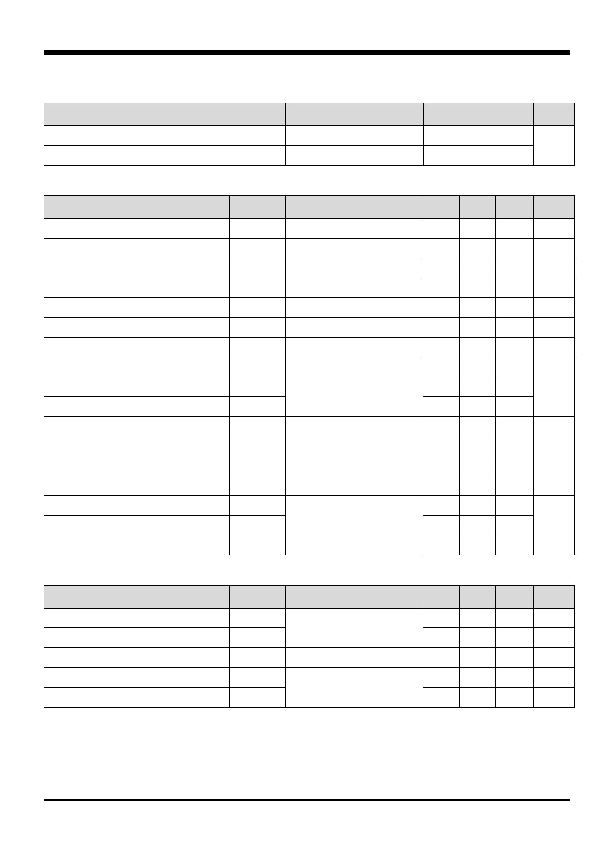
Thermal Characteristics
Characteristic
Thermal resistance, junction to case
Thermal resistance, junction to ambient
Symbol
Rth(j-c)
Rth(j-a)
SMK0825D
Rating
Max. 2.6
Max. 50
Unit
C/W
Electrical Characteristics (TC=25C unless otherwise noted)
Characteristic
Symbol
Test Condition
Drain-source breakdown voltage
Gate threshold voltage
Drain-source cut-off current
Gate leakage current
Drain-source on-resistance
Internal gate resistance
Forward transfer conductance (Note 3)
Input capacitance
Output capacitance
Reverse transfer capacitance
Turn-on delay time (Note 3,4)
Rise time (Note 3,4)
Turn-off delay time (Note 3,4)
Fall time (Note 3,4)
Total gate charge (Note 3,4)
Gate-source charge (Note 3,4)
Gate-drain charge (Note 3,4)
BVDSS
VGS(th)
IDSS
IGSS
RDS(ON)
RG
gfs
Ciss
Coss
Crss
td(on)
tr
td(off)
tf
Qg
Qgs
Qgd
ID=250uA, VGS=0
ID=250uA, VDS=VGS
VDS=250V, VGS=0V
VDS=0V, VGS=30V
VGS=10V, ID=4A
f=1MHz, VDS=0V
VDS=10V, ID=4A
VDS=25V, VGS=0V,
f=1MHz
VDD=125V, ID=8A
RG=25Ω
VDS=200V, VGS=10V
ID=8A
Min. Typ. Max. Unit
250
-
-
V
2
-
4
V
-
-
1
uA
-
- 100 nA
- 0.35 0.43
-
4
10
-
7
-
S
-
619 773
-
141 176
pF
-
33
41
11 15 35
32 85 115
ns
62 90 135
41 65 98
- 14.5 18.2
-
4
-
nC
-
4.5
-
Source-Drain Diode Ratings and Characteristics (TC=25C unless otherwise noted)
Characteristic
Symbol
Test Condition
Min. Typ. Max.
Source current (DC)
Source current (Pulsed)
Forward voltage
Reverse recovery time (Note 3,4)
Reverse recovery charge (Note 3,4)
IS
Integral reverse diode
ISM
in the MOSFET
VSD
VGS=0V, IS=8A
trr
IS=8A, VGS=0V
Qrr
dIF/dt=100A/us
-
-
8
-
-
32
-
-
1.4
-
178
-
- 1.16 -
Note:
1. Repeated rating: Pulse width limited by maximum junction temperature
2. L=8.9mH, IAS=8A, VDD=50V, RG=25, Starting TJ=25C
3. Pulse test: Pulse width≤300us, Duty cycle≤2%
4. Essentially independent of operating temperature typical characteristics
Unit
A
A
V
ns
uC
Rev. date: 12-AUG-11
KSD-T6O031-001
www.auk.co.kr
2 of 8
Share Link: 