SN71052 데이터 시트보기 (PDF) - Kodenshi Auk Co., LTD
부품명
상세내역
제조사
SN71052
Kodenshi Auk Co., LTD

SN71052 Datasheet PDF : 6 Pages
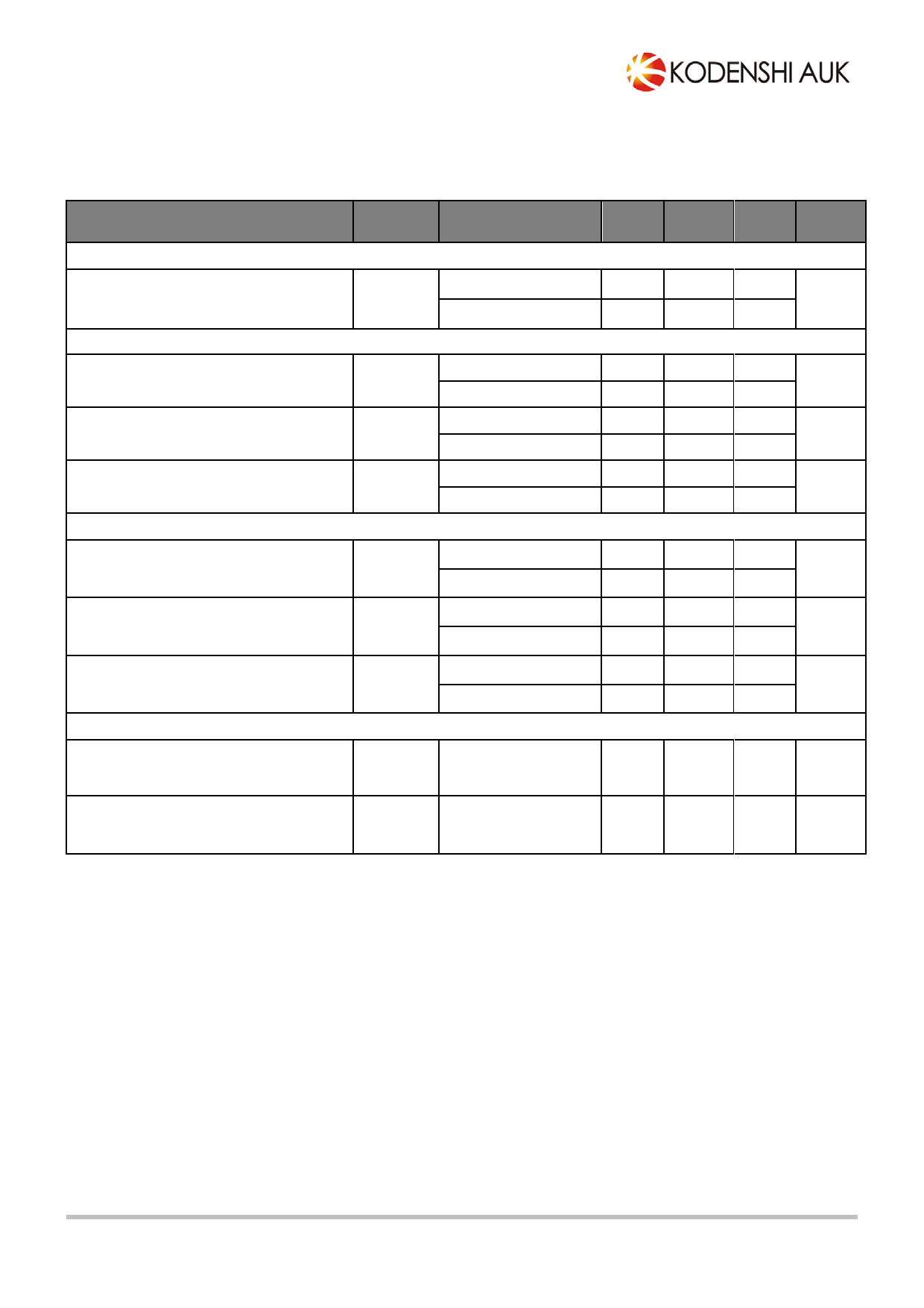
| |||
SN71052
◈ Electrical characteristics
( VCC=+5V, TA=25℃ ; unless otherwise specified )
Characteristic
Symbol Test Condition
[Total Current Consumption]
Quiescent Current
[ Voltage Control Loop OP-AMP ]
Transconductance Gain
Sink Current Only (1)
Voltage Control Loop Reference (2)
Inverting Input Bias Current
[Current Control Loop]
Transconductance Gain
sink Current Only (3)
Current Loop Reference (4)
Current out of pin ICTRL at -100mV
[Output Stage]
Low output Voltage at 10mA
Sink current
Ta = 25℃
ICC
0 < Ta < 85℃
Ta = 25℃
Gmv
0 < Ta < 85℃
Ta = 25℃
Vref
0 < Ta < 85℃
Ta = 25℃
libv
0 < Ta < 85℃
Gmi
Vsense
Iibi
Ta = 25℃
0 < Ta < 85℃
Iout = 2.5 ㎃, Ta = 25℃
0 < Ta < 85℃
Ta = 25℃
0 < Ta < 85℃
Vol
-
Output Short Circuit Current.
Output to VCC. Sink Current Only
Ios
-
Min.
-
-
1
-
1.198
1.186
-
-
1.5
-
97
96
-
-
-
-
Typ.
0.8
1.5
3.0
2.5
1.210
1.210
40
100
7.0
-
100
-
25
30
200
35
Max. Unit
2
㎃
-
-
-
1.222
1.234
-
-
㎃/㎷
V
㎁
-
㎃/㎷
-
103
㎷
104
-
㎂
-
-
㎷
70
㎃
1) If the voltage on VCTRL (the negative input of the amplifier) is higher than the positive amplifier input
(Vref = 1.210V), and it is increased by 1mV, the sinking current at the output OUT will be increased by 3.5mA.
2) The internal voltage reference is set at 1.210V (band-gap reference). The voltage control loop precision takes
into account the cumulative effects of the internal voltage reference deviation as well as the input offset voltage of the
trans-conductance operational amplifier. The internal voltage reference is fixed by band-gap, and trimmed to 0.5%
accuracy at room temperature.
3) When the positive input at ICTRL is lower than -100mV, and the voltage is decreased by 1mV, the sinking
Current at the output OUT will be increased by 7mA.
4) The internal current sense threshold is set to -100mV. The current control loop precision takes into account the cumulative
effects of the internal voltage reference deviation as well as the input offset voltage of the trans-conduction operational
amplifier.
KSD-I5P012-000
4
Dec, 2011 REV. 00
Share Link: