SP2526A 데이터 시트보기 (PDF) - Signal Processing Technologies
부품명
상세내역
제조사
SP2526A Datasheet PDF : 10 Pages
| |||
ABSOLUTE MAXIMUM RATINGS
These are stress ratings only and functional operation of the device at these ratings or any other above those indicated
in the operation sections of the specifications below is not implied. Exposure to absolute maximum rating conditions
for extended periods of time may affect reliability.
Supply Voltage(VIN)..........................................7.0V
Fault Flag Voltage (VFLG)..................................7.0V
Fault Flag Current (IFLG)..................................50mA
Enable Control Input (VEN).....................-0.3V -15V
Operating Temperature Range.............-40˚C to +85˚C
Junction Temperature Range..............................125˚C
Storage Temperature Range..............-65˚C to +150˚C
Lead Temperature (10 sec. soldering)................260˚C
Power Dissipation Per Package
8-pin NSOIC (derate 6.14mW/OC above +70OC).......500mW
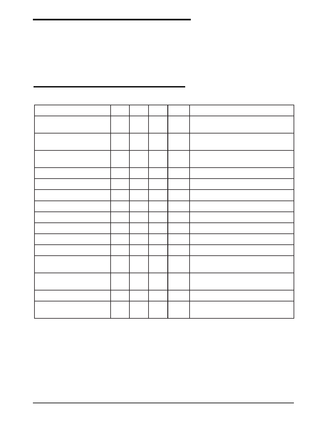
ELECTRICAL CHARACTERISTICS
Unless otherwise noted, the following specifications apply for VIN = +5.0V, TA = 25°C.
PARAMETER
Supply Current
Enable Input Voltage
Enable Input Current
Enable Input Capacitance
Output Mosfet Resistance
Output Turn-On Delay
Output Turn-On Rise Time
Output Turn-Off Delay
Output Turn-Off Fall Time
Output Leakage Current
Current Limit Threshold
Over-Temperature Shutdown
Threshold
Error Flag Output Resistance
Error Flag Off Current
UVLO Threshold
MIN. TYP. MAX. UNITS
CONDITIONS
0.75 5.0
110 160
1.7 0.8
2.4 2.0
0.01 1
0.01 1
1
µA
VEN = Logic "0" OUT = Open
VEN = Logic "1" OUT = Open
V
VEN = Logic "0"
VEN = Logic "1"
µA
VEN = Logic "0"
VEN = Logic "1"
pF
110 150 mΩ
100
1000 4000
0.8 20
0.7 20
10
µs RL=10Ω each output
µs RL=10Ω each output
µs RL=10Ω each output
µs RL=10Ω each output
µA
0.6 1.0 1.25
A
135
125
10 25
15 40
0.01 1
2.6
2.4
OC
TJ increasing
TJ decreasing
Ω
VIN = 5V,IL = 10mA
VIN = 3.3V,IL = 10mA
µA
VFLAG = 5V
V
VIN increasing
VIN decreasing
Date: 12/06/04
SP2526A Dual USB High-Side Power Switch
2
© Copyright 2004 Sipex Corporation
Share Link: 