LA9520V 데이터 시트보기 (PDF) - SANYO -> Panasonic
부품명
상세내역
제조사
LA9520V Datasheet PDF : 12 Pages
| |||
LA9520V
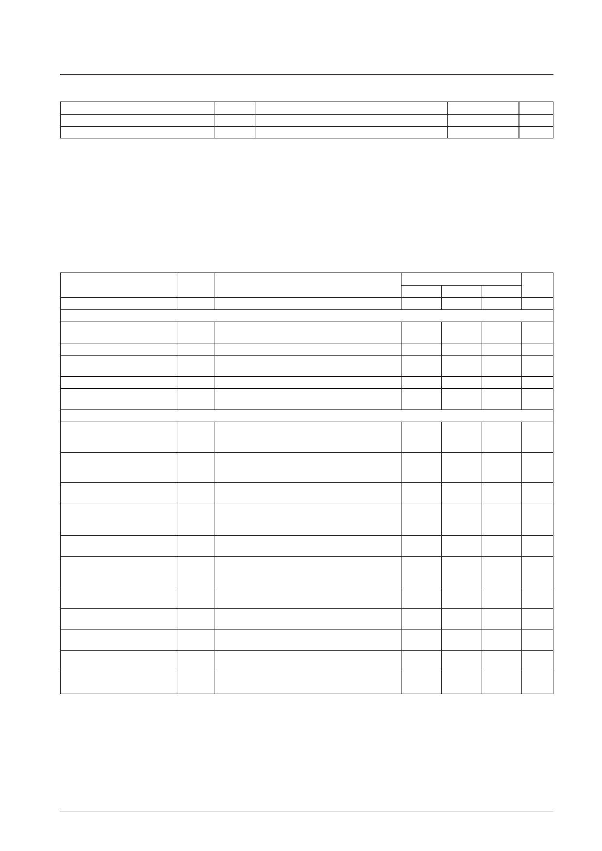
Operating Conditions at Ta = 25°C
Parameter
Recommended supply voltage
Allowable operating voltage range
Symbol
VCC
VCC opg
Conditions
Ratings
Unit
5.0
V
4.8 to 6.0
V
Electrical Characteristics at Ta = 25°C, VCC = 5 V
Representative input conditions: Carrier input frequency - Audio left channel: 4.3 MHz
Audio right channel: 4.8 MHz
Video: 11.8 MHz
Audio modulation frequency: fm = 400 Hz, 1 kHz, modulation ∆f = ±22.5 kHz (standard), ±75 kHz
Video signal input: Modulation of 2 MHz (standard) for a 0.5 Vp-p NTSC composite video signal
With the circuit adjusted to an audio demodulated output of 300 mVrms and a video demodulated output of
1 Vp-p for the above standard input.
Parameter
Symbol
Conditions
Current drain
ICC No input, VCC = 5 V, Test pins: 3, 7, 2, 5, and 32
[Preamplifier Block] *An unmodulated carrier input is used for preamplifier block testing.
Preamplifier frequency
characteristics
Input impedance
Fpre
Zin
Pin 9 input. The –3 dB frequency band,
f = 11.8 MHz, VIN = 70 dBµ, Test pin: 31
Pin 9 internal voltage conversion resistor, Test pin: 9
Output level
Voutpre
The output level when the AGC is on, VIN = 100 dBµ,
Test pin: 31
Gain (AGC off)
Harmonic distortion 1
Gvpre
TH1Pre
f = 11.8 MHz, VIN = 70 dBµ, Test pin: 31
The second harmonic of 12.5 MHz, VIN = 100 dBµ,
Test pin: 31
[Video Block]
Video amplifier gain adjustment
voltage
Demodulator linearity
Demodulator demodulation
leakage
Demodulator second harmonic
distortion
Demodulator conversion output
Video amplifier gain
Video harmonic distortion 1
Vvcont
Pin 9 input. For a 2 MHz modulated input,
The voltage such that the pin 1 output level becomes 1 Vp-p,
VIN = 100 dBµ, Test pin: 35
Pin 36 input. The conversion voltage ratio linearity at the
LINdeomo points ±3.5 MHz from the 12.5 MHz reference.
VIN = 100 dBµ, Test pin: 33
Pin 36 input. The pin 33 leakage when a carrier frequency
Vleak of 12.5 MHz is applied. VIN = 100 dBµ, Test pin: 33
THD2
Pin 36 input. The second harmonic leakage level when a
carrier frequency of 12.5 MHz is applied.
VIN = 100 dBµ, Test pin: 33
Pin 36 input. The output value when a 2 MHz modulated
Vconv. waveform is input, VIN = 100 dBµ, Test pin: 33
GVamp
Pin 34 input. With a 75 Ω load on pin 1, the total gain
after adjusting the output to be 1 Vp-p, f = 150 kHz.
VIN = 0.1 Vp-p, Test pin: 1
THD1V
The second harmonic of 150 kHz, VIN = 0.1 Vp-p
Test pin: 1
Video harmonic distortion 2
THD2V
The second harmonic of 11 MHz, VIN = 0.1 Vp-p
Test pin: 1
Video driver frequency
characteristics
Fvamp
The gain ratio for 150 kHz and 5 MHz. VIN = 0.1 Vp-p
Test pin: 1
Driver maximum output voltage
Voutmax
VCC = 5 V, the maximum output amplitude
with a 75 Ω load. Test pin: 1
DC clamp level difference
The difference between the pin 4 and the pin 5 voltages
VCLMP with no input. Test pins: 4 and 5
min
45
0.3
0.55
17
0.05
–7
0.1
–6
1.2
0.05
Ratings
typ
68
Unit
max
83 mA
20
MHz
0.5
1.0
kΩ
0.9
1.5 Vp-p
23
29
dB
–40
dB
1.15 Vdc
0
+7
%
–50
dB
–55
dB
0.23
0.4 Vp-p
13
dB
–50
dB
–48
dB
–3
+3
dB
1.5
Vp-p
0.5
Vdc
Continued on next page.
No. 6469-2/12
Share Link: 