SPX5205M5-12 데이터 시트보기 (PDF) - Signal Processing Technologies
부품명
상세내역
제조사
SPX5205M5-12 Datasheet PDF : 8 Pages
| |||
ABSOLUTE MAXIMUM RATINGS
Thermal Shutdown .................................................................... Internally Limited
Lead Temperature (Soldering, 5 seconds) ................................................. 260°C
Operating Junction Temperature Range .................................... -40°C to +125°C
Input Supply Voltage ......................................... -20V to +20V
Enable Input Voltage ......................................... -20V to +20V
RECOMMENDED OPERATING CONDITIONS
Input voltage ..................................................................................... +2.5V to 16V
Operating Junction Temperature Range .................................... -40°C to +125°C
Enable Input Voltage .............................................................................. 0V to VIN
SOT-23-5 (θJA) ................................................................................... See Note 1
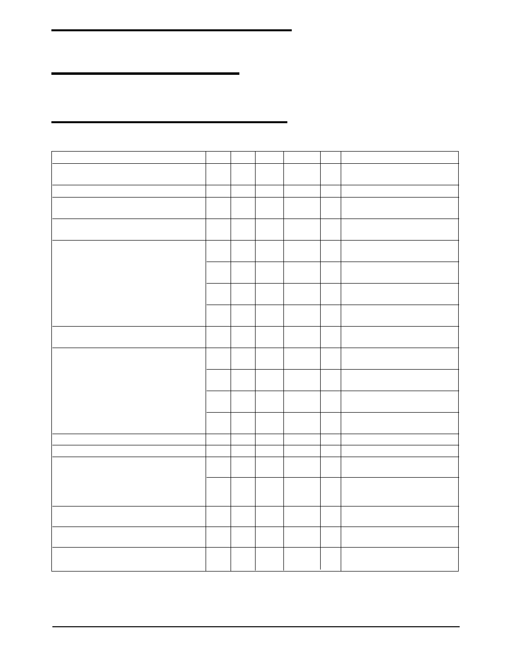
ELECTRICAL CHARACTERISTICS
TJ=25°C, VIN = VOUT + 1V, IL = 100µA, CL = 1µF, and VENABLE ≥ 2.4V. The ♦ denotes the specifications which
apply over full temperature range -40°C to +85°C, unless otherwise specified.
PARAMETER
MIN TYP MAX UNITS
Output Voltage Tolerance (VOUT)
-1
-2
+1 %VNOM
+2
Output Voltage Temperature Coefficient
57
ppm/°C
Line Regulation
0.03 0.1 %/V
0.2
Load Regulation
0.1 0.2
%
0.5
Dropout Voltage (See Note 2)
(VIN - VO)
30 50
mV
70
140 190 mV
230
180 250 mV
300
210 275 mV
350
Quiescent Current (IGND)
0.05 1
µA
5
Ground Pin Current
(IGND)
70 125
µA
150
350 600
800
750 1000
1500
1300 1900
2500
Ripple Rejection (PSRR)
70
dB
Current Limit (ILIMIT)
Output Noise (eNO)
360 500
300
mA
µVRMS
40
µVRMS
CONDITIONS
♦
♦
VIN = VOUT + 1V to 16V
♦
IL = 0.1mA to 150mA
♦
IL = 100µA
♦
IL = 50mA
♦
IL = 100mA
♦
IL = 150mA
♦
VENABLE ≤ 0.4V
♦ VENABLE ≤ 0.25V
IL = 100µA
♦
IL = 50mA
♦
IL = 100mA
♦
IL = 150mA
♦
VOUT = 0V
IL = 10mA, CL = 1µF, CIN= 1µF
(10Hz - 100kHz.)
IL = 10mA, CL = 10µF, CBYP =
1µF,CIN=1µF,(10Hz - 100kHz)
Input Voltage Level
Logic Low (VIL)
Input Voltage Level
Logic High (VIL)
ENABLE Input Current
0.4
V
2.0
0.01 2
µA
3 20
OFF
ON
VIL ≤ 0.4V
VIH ≥ 2.0V
Note 1: The maximum allowable power dissipation is a function of maximum operating junction temperature, TJ (max), the junction to ambient thermal
resistance, and the ambient, θJA, and the ambient temperature TA. The maximum allowable power dissipation at any ambient temperature is
given: PD (max) = (TJ (max) - TA)/θJA, exceeding the maximum allowable power limit will result in excessive die temperature; thus, the
regulator will go into thermal shutdown. The θJA of the SPX5205 is 220°C/W mounted on a PC board.
Note 2: Not applicable to output voltages of less than 2V.
Date:12/18/04
SPX5205 150mA, Low Noise LDO Voltage Regulator
2
© Copyright 2004 Sipex Corporation
Share Link: 