CMX624 데이터 시트보기 (PDF) - MX-COM Inc
부품명
상세내역
제조사
CMX624 Datasheet PDF : 25 Pages
| |||
Bell 202 and V.23 Compatible Modem
10
CMX624 Preliminary Information
4.8 Rx Energy and 2100Hz Detector
The Rx Energy and 2100Hz Detector functional blocks are controlled by Bit 4 and Bit 5 of the FSK MODE
Register and Bit 0 of the TX TONES Register.
This block will measure the frequency and amplitude of the incoming signal when Bit 0 of the TX TONES
Register and Bit 4 and Bit 5 of the FSK MODE Register are set to ‘1’. When a signal of 2100Hz is present
and of sufficient amplitude and time, Bit 4 of the FLAGS Register is set high. See Section 6.1 for amplitude,
time and frequency limits.
When Bit 0 of the TX TONES Register is set to ‘0’, this block compares the signal level at the output of the
Receive Filter against an internal threshold. This may be used as a FSK level detector or a simple Call
Progress Signal detector, according to the settings of Bit 4 and Bit 5 of the FSK MODE Register, which affect
the Receive Filter pass band as described in Section 4.5.
The required register settings are summarized in Table 5.
TX TONES Reg
Bit 0
0
0
0
1
FSK MODE Reg
Bit 5
Bit 4
0
0
1
0
1
1
1
1
Detection Mode
Call Progress
75 / 150bps FSK
1200bps FSK
2100Hz
Table 5: Required Register Settings
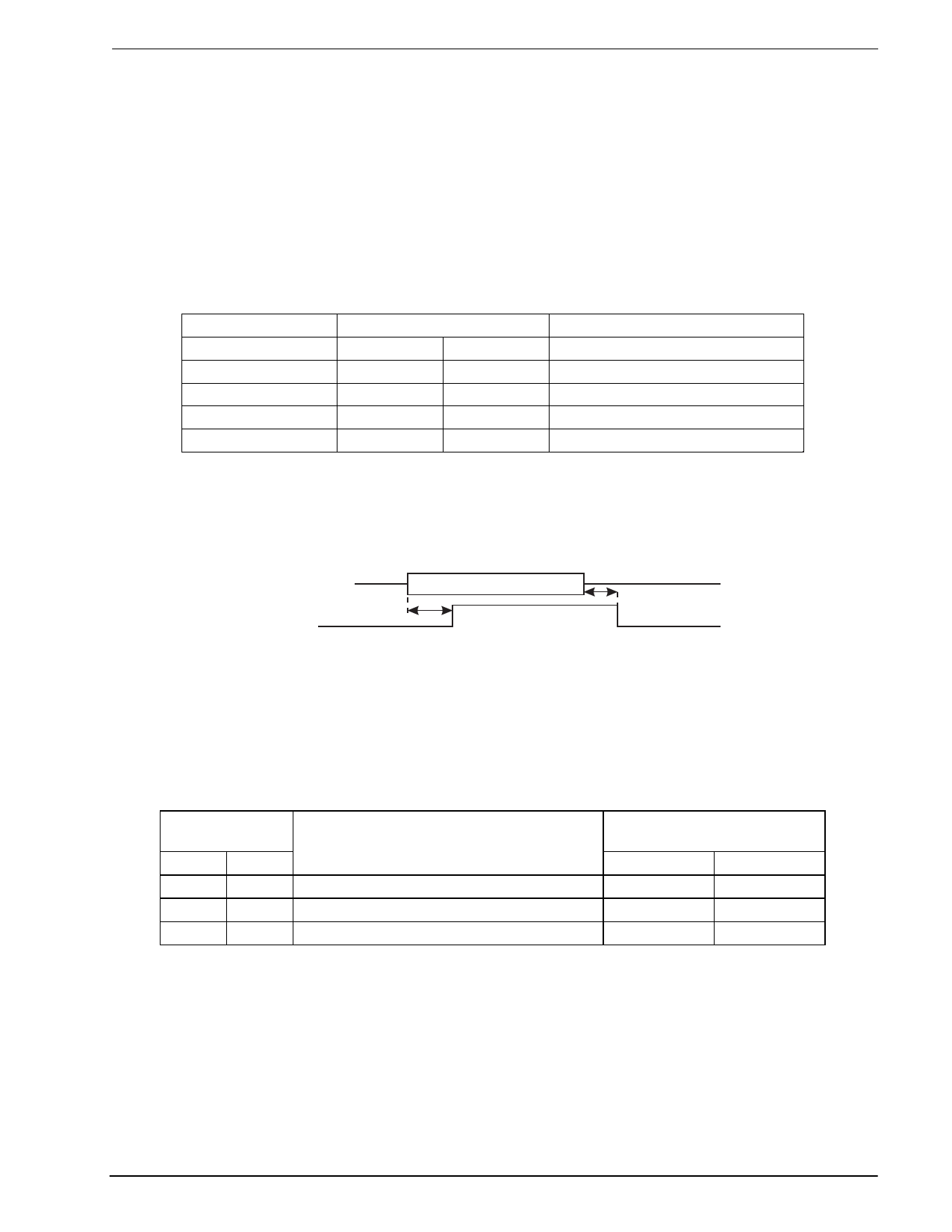
Bit 4 of the FLAGS Register is set to ‘1’ by the output of this block when the received level has exceeded the
threshold for sufficient time. Amplitude and time hysteresis, are used to reduce chattering in marginal
conditions. See Section 6.1.
Received
Line Signal
B4 of FLAGS TeON
Register
FSK or Call Progress Signal
TeOFF
Figure 8: Rx Energy Detector Timing
4.9 FSK / DTMF Modulator
When Bit 7 of the TX TONES Register is set to ‘0’ then the FSK/DTMF Modulator generates FSK signals as
determined by Bit 0 and Bit 1 of the FSK MODE Register and the Tx data bits from the UART block as shown
in Table 6 and Table 7.
4.9.1 V.23 mode (Bit 7 of SETUP register = ‘0’):
FSK MODE
Reg
Bit 1 Bit 0
0
x
1
0
1
1
FSK / DTMF Modulator block output
(Bit 7 of TX TONES = ‘0’)
Disabled (output held at VDD/2)
75bps FSK
1200bps FSK
FSK Signal Frequency
‘0’ (Space) ‘1’ (Mark)
450Hz
2100Hz
390Hz
1300Hz
Table 6: V.23 mode (Bit 7 of SETUP register = ‘0’)
©1999 MX-COM, Inc.
www.mxcom.com Tel: 800 638 5577 336 744 5050 Fax: 336 744 5054
Doc. # 20480180.108
4800 Bethania Station Road, Winston-Salem, NC 27105-1201 USA
All trademarks and service marks are held by their respective companies.
Share Link: 