CMX624 데이터 시트보기 (PDF) - MX-COM Inc
부품명
상세내역
제조사
CMX624 Datasheet PDF : 25 Pages
| |||
Bell 202 and V.23 Compatible Modem
7
4.2 Software Description
CMX624 Preliminary Information
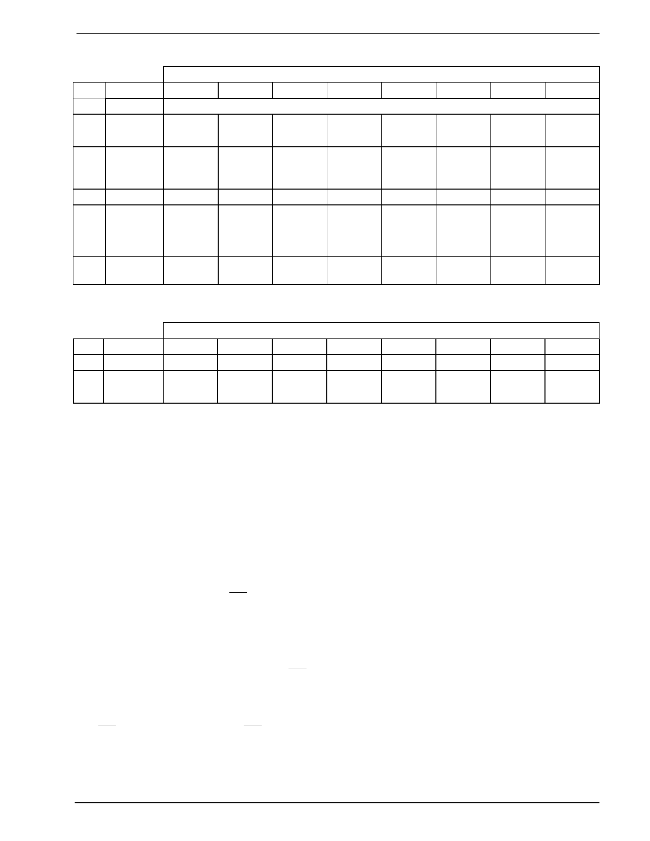
Addr
$01
$E0
$E1
$E3
$E7
Reg.
RESET
SETUP
TX
TONES
TX DATA
FSK
MODE
Command Data Byte Bits
7
6
5
4
3
2
SINGLE BYTE COMMAND
FSK mode:
0 = V.23
1 = Bell 202
Tx Mode:
0 = FSK.
1 = Tones.
D7
TX- output:
0 = Off
1 = On
Tone or
FSK output:
0 = Off.
1 = On.
D6
Relay Drive:
0 = o/c
1 = Pull low
Reserved,
set to 0
D5
0 = Zero
Power
1 = Normal
0 = DTMF
1 = Single
tone
D4
Stop bits:
0 = 1 bit
1 = 2 bits
Reserved,
set to 0
D3
Parity:
0 = None
1 = Parity
Reserved,
set to 0
D2
0 = Rx Sync
1 = Async
Rx Equal:
0 = Off
1 = On
0 = Rx Call
Progress
1 = Rx FSK
0 = Rx 75 / 0 = Tx Sync
150bps 1 = Async
1 = RX1200
Tx output
level:
0 = Normal
1 = +3dB
$EE IRQ
MASK
Reserved, Reserved, Ring Detect Reserved,
Set to 0
Set to 0
Change
Set to 0
Rx Data
overflow
Rx Data
ready
1
Parity:
0 = Odd
1 = Even
Reserved,
set to 0
D1
FSK
Enable:
0 = Off
1 = On
(Tx & Rx)
Tx Data
underflow
0
Data bits:
0 = 8 bits
1 = 7 bits
Set Detect:
0 = FSK/CP
1 = 2100Hz
D0
0 = Tx 75 /
150bps
1 = 1200 or
DTMF
Tx Data
ready
Table 2: Write Only Serial Bus Register
Addr Reg.
$EA RX DATA
$EF FLAGS
7
D7
Bad Rx
Parity
** See note 2 and 3
Reply Data Byte Bits
6
5
4
3
D6
D5
D4
D3
Ring Detect Ring Detect Rx Energy
Change ** or 2100Hz
detect.
Rx Data
overflow **
2
D2
Rx Data
ready **
1
D1
Tx Data
underflow **
Table 3: Read Only Serial Bus Registers
0
D0
Tx Data
ready **
Notes:
1. Accessing the RESET Register over the Serial Bus clears all of the bits in the SETUP, TX TONES, TX
DATA, FSK MODE and IRQ MASK registers, and Bits 0-3 and Bit 5 of the FLAGS Register to ‘0’. This
will set the device into Zero Power mode.
a) This is a single-byte Serial Bus transaction consisting solely of the address byte value $01.
b) Placing the device in Zero Power mode by directly setting SETUP Bit 4 to ‘0’ does not clear the other
register bits. Care should be taken before re-enabling the device that the other bits are set so as to
prevent undesired transient operation. In particular, bit 6 of the TXTONES Register should be set to
‘0’ to prevent modulation of the transmitter output.
2. If any of Bits 0, 1, 2, 3 or 5 of the FLAGS Register is ‘1’ and the corresponding bit of the IRQ MASK
Register is also ‘1’ then the IRQ output of the CMX624 will be pulled low.
3. Bit 5 (Ring Detect Change) of the FLAGS Register is set on every ‘0’ to ‘1’ or ‘1’ to ‘0’ change of Bit 6
(Ring Detect).
4. Clearing Bit 4 of the SETUP Register puts the CMX624 into the Zero Power mode by turning off all blocks
except for the Serial Bus interface and Ring Detector circuit.
5. Reading the FLAGS Register clears the IRQ output and also clears Bits 0, 1, 2, 3 and 5 of the FLAGS
Register.
6. FLAGS Register (bit 4) is ‘1’ whenever Rx Energy or 2100Hz are present and ‘0’ when both signals are
absent. IRQ Mask Register (bit 40 is normally set to ‘0’, but can be set to ‘1’ to enable interrupts on the
IRQ output. In the latter case, IRQ will be continuously pulled to ’0’ while Rx Energy or 2100Hz are
present. This may be useful for device evaluation purposes.
©1999 MX-COM, Inc.
www.mxcom.com Tel: 800 638 5577 336 744 5050 Fax: 336 744 5054
Doc. # 20480180.108
4800 Bethania Station Road, Winston-Salem, NC 27105-1201 USA
All trademarks and service marks are held by their respective companies.
Share Link: 