SST25VF016B 데이터 시트보기 (PDF) - Silicon Storage Technology
부품명
상세내역
제조사
SST25VF016B Datasheet PDF : 28 Pages
| |||
16 Mbit SPI Serial Flash
SST25VF016B
Block Protection (BP3,BP2, BP1, BP0)
The Block-Protection (BP3, BP2, BP1, BP0) bits define the
size of the memory area, as defined in Table 4, to be soft-
ware protected against any memory Write (Program or
Erase) operation. The Write-Status-Register (WRSR)
instruction is used to program the BP3, BP2, BP1 and BP0
bits as long as WP# is high or the Block-Protect-Lock
(BPL) bit is 0. Chip-Erase can only be executed if Block-
Protection bits are all 0. After power-up, BP3, BP2, BP1
and BP0 are set to 1.
Data Sheet
Block Protection Lock-Down (BPL)
WP# pin driven low (VIL), enables the Block-Protection-
Lock-Down (BPL) bit. When BPL is set to 1, it prevents any
further alteration of the BPL, BP3, BP2, BP1, and BP0 bits.
When the WP# pin is driven high (VIH), the BPL bit has no
effect and its value is “Don’t Care”. After power-up, the BPL
bit is reset to 0.
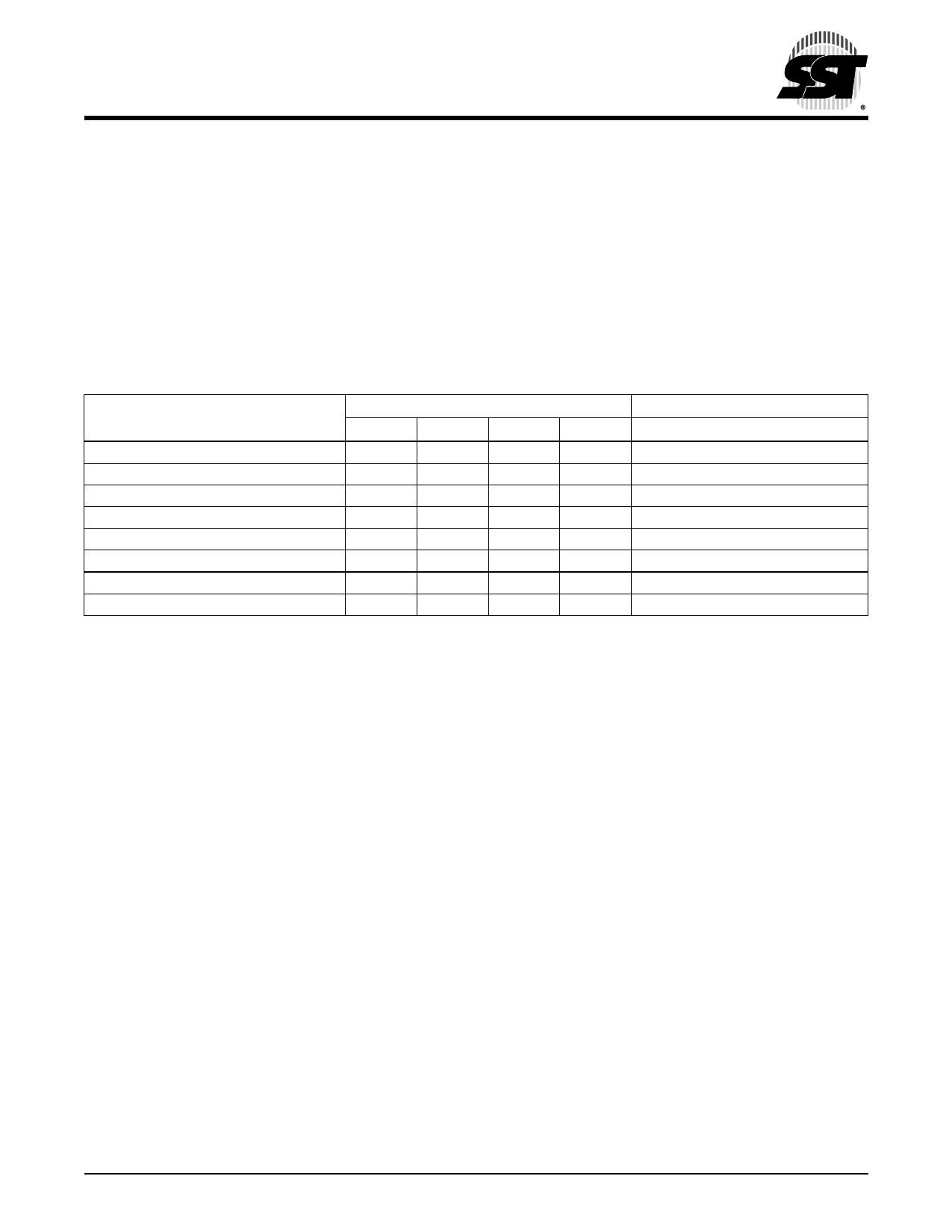
TABLE 4: Software Status Register Block Protection FOR SST25VF016B1
Status Register Bit2
Protection Level
BP3
BP2
BP1
BP0
None
X
0
0
0
Upper 1/32
X
0
0
1
Upper 1/16
X
0
1
0
Upper 1/8
X
0
1
1
Upper 1/4
X
1
0
0
Upper 1/2
X
1
0
1
All Blocks
X
1
1
0
All Blocks
X
1
1
1
1. X = Don’t Care (RESERVED) default is “0
2. Default at power-up for BP2, BP1, and BP0 is ‘111’. (All Blocks Protected)
Protected Memory Address
16 Mbit
None
1F0000H-1FFFFFH
1E0000H-1FFFFFH
1C0000H-1FFFFFH
180000H-1FFFFFH
100000H-1FFFFFH
000000H-1FFFFFH
000000H-1FFFFFH
T4.0 1271
©2008 Silicon Storage Technology, Inc.
7
S71271-03-000
9/08
Share Link: 