SST37VF010 데이터 시트보기 (PDF) - Silicon Storage Technology
부품명
상세내역
제조사
SST37VF010
Silicon Storage Technology

SST37VF010 Datasheet PDF : 16 Pages
| |||
512 Kbit / 1 Mbit / 2 Mbit / 4 Mbit Multi-Purpose Flash
SST37VF512 / SST37VF010 / SST37VF020 / SST37VF040
Data Sheet
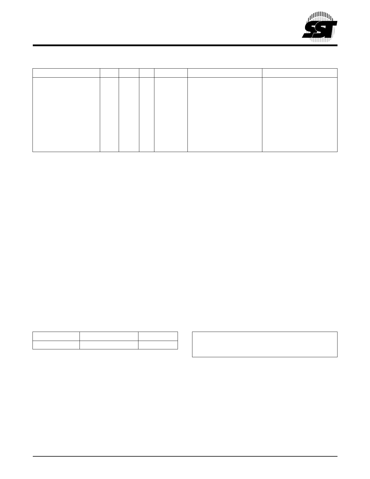
TABLE 3: OPERATION MODES SELECTION
Mode
CE# WE# A9
OE# DQ
Address
Read
VIL
VIH AIN
VIL
DOUT
AIN
Output Disable
VIL
X
X
VIH
High Z
AIN
Standby
VIH
X
X
X
High Z
X
Chip-Erase
VIL
VIL VH
VH
High Z
X
Byte-Program
VIL
VIL AIN
VH
DIN
AIN
Program/Erase Inhibit
X
VIH
X
X
High Z
X
Product Identification
X
X
X VIL or VIH High Z/ DOUT
VIL
VIH VH
VIL
Manufacturer’s ID (BFH)
Device ID1
X
AMS2 - A1 = VIL, A0 = VIL
AMS2 - A1 = VIL, A0 = VIH
1. Device ID = C4H for SST37VF512, C5H for SST37VF020, C6H for SST37VF020, and C2H for SST37VF040
2. AMS = Most significant address
AMS = A15 for SST37VF512, A16 for SST37VF010, A17 for SST37VF020, and A18 for SST37VF040
Note: X = VIL or VIH (or VH in case of OE# and A9)
VH = 12V±5%
T3.1 397
Absolute Maximum Stress Ratings (Applied conditions greater than those listed under “Absolute Maximum
Stress Ratings” may cause permanent damage to the device. This is a stress rating only and functional operation
of the device at these conditions or conditions greater than those defined in the operational sections of this data
sheet is not implied. Exposure to absolute maximum stress rating conditions may affect device reliability.)
Temperature Under Bias . . . . . . . . . . . . . . . . . . . . . . . . . . . . . . . . . . . . . . . . . . . . . . . . . . . . . . . . . -55°C to +125°C
Storage Temperature . . . . . . . . . . . . . . . . . . . . . . . . . . . . . . . . . . . . . . . . . . . . . . . . . . . . . . . . . . . -65°C to +150°C
D. C. Voltage on Any Pin to Ground Potential . . . . . . . . . . . . . . . . . . . . . . . . . . . . . . . . . . . . . . . -0.5V to VDD + 0.5V
Transient Voltage (<20 ns) on Any Pin to Ground Potential . . . . . . . . . . . . . . . . . . . . . . . . . . . . -1.0V to VDD + 1.0V
Voltage on A9 Pin to Ground Potential . . . . . . . . . . . . . . . . . . . . . . . . . . . . . . . . . . . . . . . . . . . . . . . . -0.5V to 13.2V
Package Power Dissipation Capability (Ta = 25°C) . . . . . . . . . . . . . . . . . . . . . . . . . . . . . . . . . . . . . . . . . . . . . . 1.0W
Through Hold Lead Soldering Temperature (10 Seconds) . . . . . . . . . . . . . . . . . . . . . . . . . . . . . . . . . . . . . . . 300°C
Surface Mount Lead Soldering Temperature (3 Seconds) . . . . . . . . . . . . . . . . . . . . . . . . . . . . . . . . . . . . . . . 240°C
Output Short Circuit Current1 . . . . . . . . . . . . . . . . . . . . . . . . . . . . . . . . . . . . . . . . . . . . . . . . . . . . . . . . . . . . . 50 mA
1. Outputs shorted for no more than one second. No more than one output shorted at a time.
OPERATING RANGE
Range
Commercial
Ambient Temp
0°C to +70°C
VDD
2.7-3.6V
AC CONDITIONS OF TEST
Input Rise/Fall Time . . . . . . . . . . . . . . . 5 ns
Output Load . . . . . . . . . . . . . . . . . . . . . CL = 100 pF
See Figures 7 and 8
©2001 Silicon Storage Technology, Inc.
5
S71151-02-000 5/01 397
Share Link: