SST37VF010 데이터 시트보기 (PDF) - Silicon Storage Technology
부품명
상세내역
제조사
SST37VF010
Silicon Storage Technology

SST37VF010 Datasheet PDF : 16 Pages
| |||
512 Kbit / 1 Mbit / 2 Mbit / 4 Mbit Multi-Purpose Flash
SST37VF512 / SST37VF010 / SST37VF020 / SST37VF040
Data Sheet
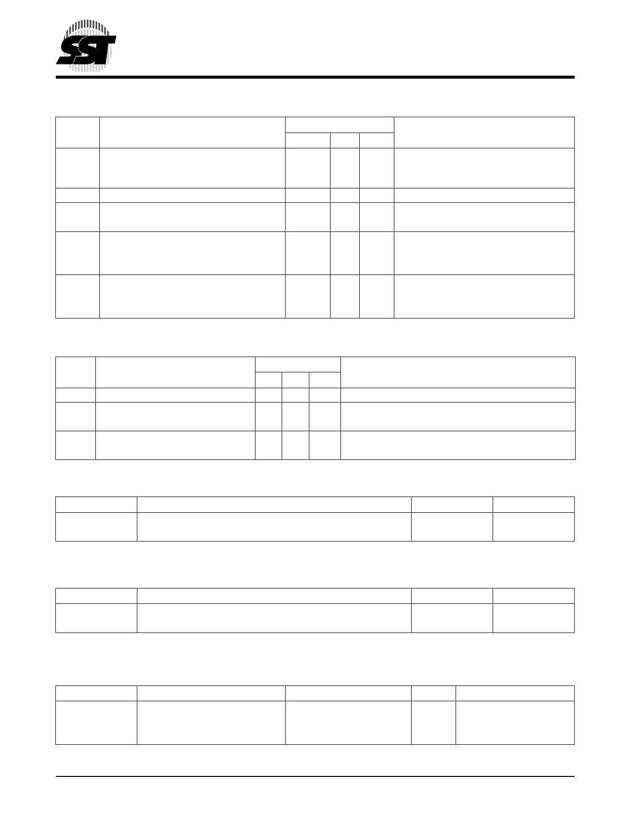
TABLE 4: READ MODE DC OPERATING CHARACTERISTICS VDD=2.7-3.6V (Ta = 0°C to +70°C (Commercial))
Limits
Symbol Parameter
Min Max Units Test Conditions
IDD
ISB
ILI
ILO
VIL
VIH
VIHC
VOL
VOH
IH
VDD Read Current
Standby VDD Current
Input Leakage Current
Output Leakage Current
Input Low Voltage
Input High Voltage
Input High Voltage (CMOS)
Output Low Voltage
Output High Voltage
Supervoltage Current for A9 for Read-ID
12
15
1
10
0.8
0.7 VDD
VDD-0.3
0.2
VDD-0.3
200
Address input=VIL/VIH, at f=1/TRC Min
VDD=VDD Max
mA CE#=OE#=VIL, all I/Os open
µA CE#=VIHC, VDD=VDD Max
µA VIN=GND to VDD, VDD=VDD Max
µA VOUT=GND to VDD, VDD=VDD Max
V VDD=VDD Min
V VDD=VDD Max
V VDD=VDD Max
V IOL=100 µA, VDD=VDD Min
V IOH=-100 µA, VDD=VDD Min
µA CE#=OE#=VIL, A9=VH Max
T4.3 397
TABLE 5: PROGRAM/ERASE DC OPERATING CHARACTERISTICS VDD=2.7-3.6V (Ta = 25°C±5°C)
Limits
Symbol Parameter
Min Max Units Test Conditions
IDD
VDD Erase or Program Current
20 mA CE#=VIL, OE#=VH, VDD=VDD Max, WE#=VIL
ILI
Input Leakage Current
1 µA VIN=GND to VDD, VDD=VDD Max
ILO
Output Leakage Current
10 µA VOUT=GND to VDD, VDD=VDD Max
VH
Supervoltage for A9 and OE#
11.4 12.6 V
IH
Supervoltage Current for A9 and OE#
200 µA OE#=VH Max, A9=VH Max, VDD=VDD Max, CE# = VIL
T5.1 397
TABLE 6: RECOMMENDED SYSTEM POWER-UP TIMINGS
Symbol
Parameter
Minimum
Units
TPU-READ1
TPU-WRITE1
Power-up to Read Operation
Power-up to Write Operation
100
µs
100
µs
T6.1 397
1. This parameter is measured only for initial qualification and after a design or process change that could affect this parameter.
TABLE 7: CAPACITANCE (Ta = 25°C, f=1 Mhz, other pins open)
Parameter
Description
Test Condition
Maximum
CI/O1
I/O Pin Capacitance
VI/O = 0V
12 pF
CIN1
Input Capacitance
VIN = 0V
6 pF
T7.0 397
1. This parameter is measured only for initial qualification and after a design or process change that could affect this parameter.
TABLE 8: RELIABILITY CHARACTERISTICS
Symbol
Parameter
Minimum Specification
Units Test Method
NEND1
Endurance
10,000
Cycles JEDEC Standard A117
TDR1
Data Retention
100
Years JEDEC Standard A103
ILTH1
Latch Up
100 + IDD
mA JEDEC Standard 78
T8.3 397
1. This parameter is measured only for initial qualification and after a design or process change that could affect this parameter.
©2001 Silicon Storage Technology, Inc.
6
S71151-02-000 5/01 397
Share Link: