SST39SF010A 데이터 시트보기 (PDF) - Silicon Storage Technology
부품명
상세내역
제조사
SST39SF010A Datasheet PDF : 25 Pages
| |||
1 Mbit / 2 Mbit / 4 Mbit Multi-Purpose Flash
SST39SF010A / SST39SF020A / SST39SF040
Data Sheet
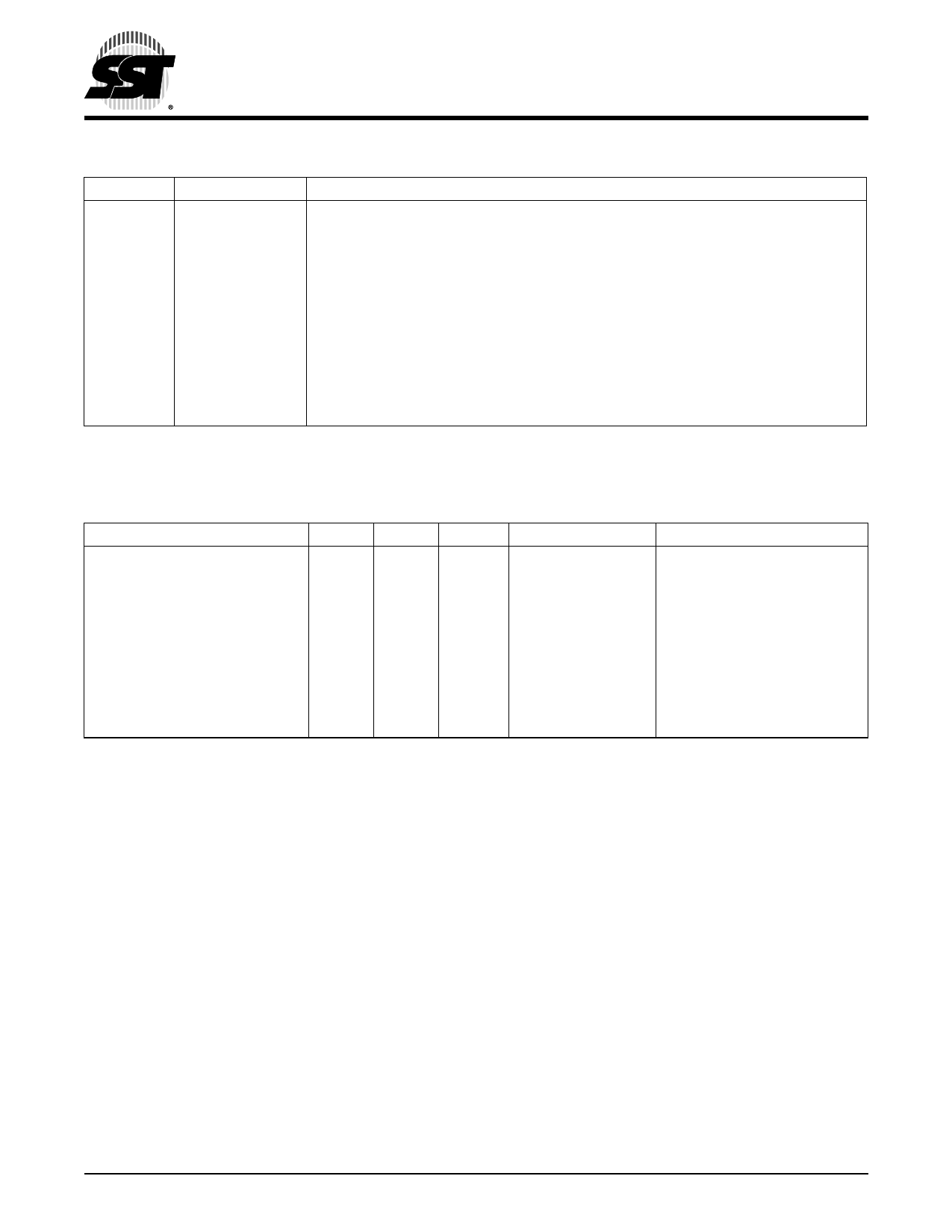
TABLE 2: Pin Description
Symbol
AMS1-A0
Pin Name
Address Inputs
DQ7-DQ0 Data Input/output
CE#
OE#
WE#
VDD
VSS
NC
Chip Enable
Output Enable
Write Enable
Power Supply
Ground
No Connection
Functions
To provide memory addresses.
During Sector-Erase AMS-A12 address lines will select the sector.
To output data during Read cycles and receive input data during Write cycles.
Data is internally latched during a Write cycle.
The outputs are in tri-state when OE# or CE# is high.
To activate the device when CE# is low.
To gate the data output buffers.
To control the Write operations.
To provide 5.0V supply (4.5-5.5V)
Unconnected pins.
1. AMS = Most significant address
AMS = A16 for SST39SF010A, A17 for SST39SF020A, and A18 for SST39SF040
T2.2 1147
TABLE 3: Operation Modes Selection
Mode
Read
Program
Erase
CE#
VIL
VIL
VIL
OE#
VIL
VIH
VIH
Standby
Write Inhibit
Product Identification
Software Mode
VIH
X
X
VIL
X
X
VIL
VIL
1. X can be VIL or VIH, but no other value.
WE#
VIH
VIL
VIL
DQ
DOUT
DIN
X1
X
High Z
X
High Z/ DOUT
VIH
High Z/ DOUT
VIH
Address
AIN
AIN
Sector address,
XXH for Chip-Erase
X
X
X
See Table 4
T3.3 1147
©2010 Silicon Storage Technology, Inc.
6
S71147-09-000
01/10
Share Link: 