ST485B 데이터 시트보기 (PDF) - STMicroelectronics
부품명
상세내역
제조사
ST485B Datasheet PDF : 19 Pages
| |||
ST485B - ST485C
Electrical characteristics
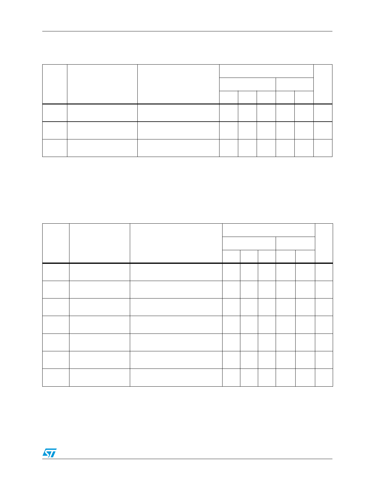
Table 6.
Symbol
DC electrical characteristics (continued)
VCC = 5 V ± 5 %, TA = TMIN to TMAX, unless otherwise specified. Typical values are referred
to TA = 25 °C)
Value
Parameter
Test conditions (1)
-40 to 85 °C
-55 to 125 °C Unit
Min. Typ. Max. Min. Max.
IOSD1
IOSD2
IOSR
Driver short-circuit
current, VO=High
Driver short-circuit
current, VO=Low
Receiver short-circuit
current
VO = -7 to 12V (3)
VO = -7 to 12V (3)
VO = 0V to VCC
35
250 35 250 mA
35
250 35 250 mA
7
95 7 95 mA
1. All currents into device pins are positive; all cuttents out of device pins are negative; all voltages are referenced to device
ground unless specified.
2. Supply current specification is valid for loaded transmitters when VDE = 0V
3. Applies to peak current. See typical Operating Characteristics.
Table 7.
Symbol
Driver switching characteristics
VCC = 5 V ± 5 %, TA = TMIN to TMAX, unless otherwise specified. Typical values are referred
to TA = 25 °C
Value
Parameter
Test conditions (1)
-40 to 85 °C
-55 to 125°C Unit
Min. Typ. Max. Min. Max.
tPLH
tPHL
tSK
tTLH
tTHL
tPZH
Propagation delay
input to output
RDIFF = 54Ω, CL1 = CL2 = 100pF
(See Figure 4 and Figure 6)
Output skew to output
RDIFF = 54Ω, CL1 = CL2 = 100pF
(See Figure 4 and Figure 6)
Rise or fall time
RDIFF = 54Ω, CL1 = CL2 = 100pF
(See Figure 4 and Figure 6)
Output enable time
CL = 100pF, S2 = Closed
(See Figure 5 and Figure 7)
10 30 60
5 10
3 15 40 3
70 90
70 ns
10 ns
45 ns
90 ns
tPZL Output enable time
tPLZ Output disable time
tPHZ Output disable time
CL = 100pF, S1 = Closed
(See Figure 5 and Figure 7)
CL = 15pF, S1 = Closed
(See Figure 5 and Figure 7)
CL = 15pF, S2 = Closed
(See Figure 5 and Figure 7)
70 90
70 90
70 90
90 ns
90 ns
90 ns
1. All currents into device pins are positive; all cuttents out of device pins are negative; all voltages are referenced to device
ground unless specified.
7/19
Share Link: 