STK681-332-E-D 데이터 시트보기 (PDF) - SANYO -> Panasonic
부품명
상세내역
제조사
STK681-332-E-D Datasheet PDF : 14 Pages
| |||
STK681-332-E
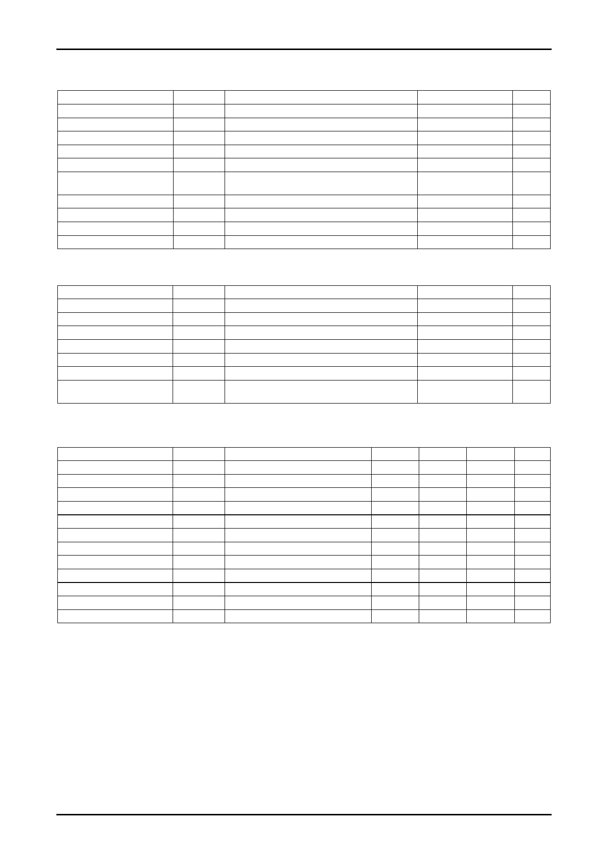
Specifications
Absolute maximum ratings at Tc = 25°C
Parameter
Maximum supply voltage 1
Maximum supply voltage 2
Input voltage
Output current1
Output current2
Brake current
Symbol
VCC max
VDD max
VIN max
IO1 max
IO2 max
IOB max
Allowable power dissipation
Operating substrate temperature
Junction temperature
Storage temperature
PdPK max
Tc
Tj max
Tstg
Conditions
VDD=0V
No signal
Logic input pins
VDD=5.0V, DC current
VDD=5.0V, Pulse current: 5ms
VDD=5.0V, square wave current, operating time 15ms
(single pulse, low side brake)
No heat sink
Metal surface temperature of the package
Ratings
unit
52
V
-0.3 to +6.0
V
-0.3 to +6.0
V
8.5
A
12
A
12
A
2.8
W
-20 to +105
°C
150
°C
-40 to +125
°C
Allowable Operating Ranges at Ta = 25°C
Parameter
Symbol
Conditions
Ratings
unit
Operating supply voltage 1
VCC1
With signals applied (Tc=105°C)
10 to 38
V
Operating supply voltage 2
VCC2
With signals applied (Tc=90°C)
10 to 42
V
Operating supply voltage 2
VDD
With signals applied
5±5%
V
Input voltage
Output current 1
VIN
IO1
VDD=5.0V, DC current, Tc=80°C
0 to VDD
V
6.1
A
Output current 2
IO2
VDD=5.0V, DC current, Tc=105°C
5
A
Brake current
IOB
VDD=5.0V, square wave current, operating time 2ms,
Low side brake, Tc=105°C
12
A
Refer to the graph for each conduction-period tolerance range for the output current and brake current.
Electrical Characteristics at Tc = 25°C, VCC = 24V, VDD = 5.0V
Parameter
VDD supply current
FET diode forward voltage
Output saturation voltage 1
Output saturation voltage 2
Output leak current
Input high voltage
Input low voltage
High-level input current
Low-Level Input current
Overcurrent detection voltage
Symbol
ICCO
Vdf
Vsat1
Vsat2
IOL
VIH
VIL
IILH
IILL
VOC
Conditions
Forward or reverse operation
If=1A (RL=23Ω)
RL=23Ω, F1, F2
RL=23Ω, F3, F4
F1, F2, F3, and F4 OFF operation
IN1, IN2, ENABLE pins
IN1, IN2, ENABLE pins
IN1, IN2, ENABLE pins, VIH=5V
IN1, IN2, ENABLE pins, VIL=GND
Between pins Vref1 and S.P
Internal PWM frequency
fc
Overheat detection temperature TSD
Design guarantee
Note: A fixed-voltage power supply must be used.
min
2.5
32
typ
6
0.75
65
50
50
0.48
46
144
max
unit
9
mA
1.4
V
100
mV
85
mV
50
μA
V
0.8
V
75
μA
10
μA
V
62 kHz
°C
No. A1591-2/14
Share Link: 