M52742ASP 데이터 시트보기 (PDF) - MITSUBISHI ELECTRIC
부품명
상세내역
제조사
M52742ASP Datasheet PDF : 21 Pages
| |||
PRELIMINARY NSootmicee:pTahriasmisentroict alimfiintsalasrpeescuifbicjeactitotno. change.
MITSUBISHI ICs (Monitor)
M52742ASP
BUS CONTROLLED 3-CHANNEL VIDEO PREAMP FOR CRT DISPLAY MONITOR
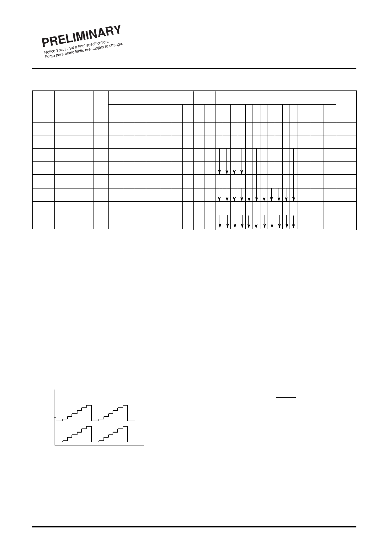
ELECTRICAL CHARACTERISTICS (cont.)
Symbol
Parameter
Test
Input
point 2,6,11 1 4,9,13 19
(s)
RGB
in
OSD
BLK
OSD
in
CP in
27 7 16
ReT SOG UNI
BLK in in
CTL
voltage
BUS CTL (H)
Limits
30
Bri-
ght
15 00H 01H 02H 03H 04H 05H 06H 07H 08H 09H 0BH
ABL Main Sub Sub Sub OSD BLK D/A D/A D/A D/A INT
cont cont cont cont Adj Adj OUT OUT OUT OUT EXT
123
1234
Min.
Typ. Max.
TDS-R
Sync output
delay time2
Sync OUT
a
aa
a
a
b
SG4
a
2.0 5.0
0 60 90
VOH
D/A H output
voltage
D/A
OUT
a
aa
a
a
a
a 2.0 5.0 4.5 5.0 5.5 FFH FFH FFH FFH 00H 00H FFH FFH FFH FFH 00H
255 255 255 255 0 0 255 255 255 255 0
VOL
D/A L output
voltage
D/A
OUT
a
aa
a
a a a 2.0 5.0
00H 00H 00H 00H
0000
0 0.5 1.0
DNL
UNI1
UNI2
D/A
nonlinearity
D/A
OUT
a
a
Uniformity
characteristics1
OUT
b
SG1
a
Uniformity
characteristics2
OUT
b
SG1
a
aaa
a
b
SG5
a
a
b
SG5
a
a a 2.0 5.0
b
a
2.0 5.0 SG6
2.5V
C8H C8H C8H C8H
200 200 200 200
a
b
SG6
2.0
5.0
1.25V
Vari Vari Vari Vari
able able able able
FFH FFH FFH FFH
255 255 255 255
-1.0 - 1.0
7 10 13
3.5 5 6.5
1A-
D/A input
current range
D/A
OUT
a
a
a
aa
a
a
2.0 5.0 0.18 00H 00H 00H 00H 00H 00H 00H 00H 00H 00H 00H
00 000
0
00 000
-
-
1A+
D/A output
D/A a a a
current range OUT
a a a a 2.0 5.0
- - 1.0
Unit
ns
VDC
VDC
LSB
%
%
mA
mA
ELECTRICAL CHARACTERISTICS TEST METHOD
ICC1 Circuit current1
Measuring conditions are as listed in supplementary Table.
Measured with a current meter at test point IA.
ICC2 Circuit current2
Measuring conditions are as listed in supplementary Table.
Measured with a current meter at test point IB.
Vomax Output dynamic range
Decrease V30 gradually, and measure the voltage when the
waveform output is distorted. The voltage is called VOL.
Next, increase V30 gradually, and measure the voltage when the
top of waveform output is distorted. The voltage is called VOH.
Voltage Vomax is calculated by the equation below:
Vomax = VOH-VOL
(V)
VOH
5.0
Waveform output
VOL
0.0
Gv Maximum gain
Input SG1, and read the amplitude output at OUT (29, 32, 35). The
amplitude is called VOUT (29, 32, 35). Maximum gain GV is
calculated by the equation below:
GV=20Log VOUT (dB)
0.7
∆Gv Relative maximum gain
Relative maximum gain DGV is calculated by the equation bellow:
∆GV= VOUT (29)/VOUT (32),
VOUT (32)/VOUT (35),
VOUT (35)/VOUT (29)
VC1 Main contrast control characteristics1
Measuring the amplitude output at OUT (29, 32, 35). The
measured value is called VOUT (29, 32, 35). Main contrast control
characterics VC1 is calculated by the equation bellow:
VC1=20Log
VOUT
0.7
(dB)
∆VC1 Main contrast control relative characteristics1
Relative characteristics ∆VC1 is calculated by the equation bellow:
∆VC1=VOUT (29)/VOUT (32),
VOUT (32)/VOUT (35),
VOUT (35)/VOUT (29)
Vimax Maximum input
Increase the input signal (SG2) amplitude gradually, starting from
700mVP-P. Measure the amplitude of the input signal when the
output signal starts becoming distorted.
VC2 Main contrast control characteristics2
Measuring condition and procedure are the same as described in
VC1.
∆VC2 Main contrast control relative characteristics2
Measuring condition and procedure are the same as described in
∆VC1.
6
Share Link: 