SX1223 데이터 시트보기 (PDF) - Semtech Corporation
부품명
상세내역
제조사
SX1223 Datasheet PDF : 25 Pages
| |||
SX1223
4.1.4 Charge Pump
The charge pump current can be set to either 125 or 500 µA by the CP_HI bit. The default value at power-up is 125
µA (CP_HI = ‘0’). The choice of this current affects the loop filter component values (see section 4.1.5). For most
applications the lowest current mode is recommended. For those applications using a high phase detector
frequency and a high PLL bandwidth, 500 µA may provide a better solution.
4.1.5 Loop Filter
The design of the PLL filter will strongly affect the performance of the frequency synthesizer. The PLL filter is kept
external for flexibility. The parameters to be considered when designing the loop filter for the SX1223 are primarily
the modulation mode and bit rate. These will also affect the switching time and phase noise.
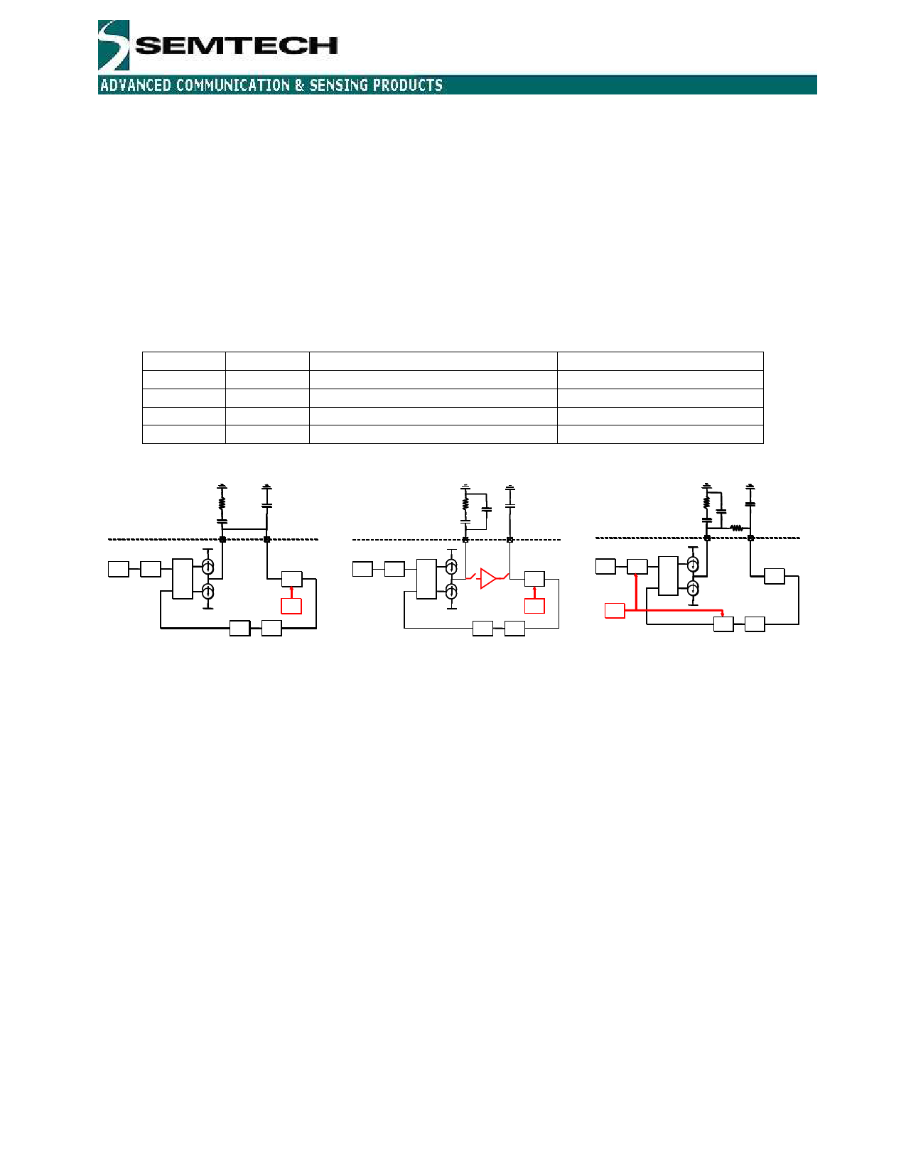
The frequency modulation can be done in three different ways with the SX1223, either by closed-, open loop VCO
modulation or by modulation with the internal dividers, see Table 3 and modulation selection guide in Table 35.
Modulation1 Modulation0 State
0
0
Closed loop VCO-modulation (mw1)
0
1
Open loop VCO-modulation (mw2)
1
0
Modulation by A,M and N (mw3)
1
1
Not used
Table 3: Modulation modes
Comments
VCO is phase-locked
VCO is free-running
Modulation inside PLL
PCB
SX1223
XCO ÷ M
R1
C2
20
PFD
C3
21
VCO
÷ N,A
MOD
÷2
PCB
SX1223
XCO ÷ M
R1
C1
C3
C2
20
21
PFD
VCO
OL opamp
MOD
÷ N,A ÷ 2
PCB
SX1223
XCO ÷ M
R1
C2
20
PFD
C3
C1
R2
21
VCO
MOD
÷ N,A ÷ 2
Modulation mw1
Modulation mw2
Modulation mw3
Figure 4: Modulation modes
In closed loop VCO modulation (mw1), the PLL bandwidth needs to be sufficiently low (≈ Bit Rate / 20), so as to
prevent the VCO tracking the modulation and cancelling the modulation.
Using the dividers in mw3 mode, the PLL needs to lock on a new carrier frequency for every new data bit. Now the
PLL bandwidth needs to be sufficiently high (≈ Bit Rate / 2). It may be necessary to implement a third order filter to
futher suppress the phase detector frequency spurs,
For the open loop VCO modulation case (mw2), the PLL bandwidth can be large, as the PLL is deactivated during
the transmission burst and there is no requirement to supress the phase detector frequency
To increase the transmission time in the open loop case, a capacitor of 47 nF can be connected on pin VARIN to
ground (NPO type is advised if the transmission duration is critical). The internal opamp must be enabled to drive
this capacitor, by setting the bit OL_opamp_en to 1.
A schematic for a third order loop filter is shown in Figure 5a. For a second order filter, C3 is not connected and R2
is set to 0 Ω. When designing a third order loop filter, the internal capacitance on the VARIN pin of approximately 6
pF must be taken into consideration. Figure 5b shows the loop filter configuration for the open loop VCO modulation
case.
© Semtech 2007
www.semtech.com
10
Share Link: 