SX1223 데이터 시트보기 (PDF) - Semtech Corporation
부품명
상세내역
제조사
SX1223 Datasheet PDF : 25 Pages
| |||
SX1223
The SX1223 is a single chip transmitter operating in the 433, 868 and 915MHz license free ISM (Industrial Scientific
and Medical) frequency bands; the frequency range is selectable between 425-475 MHz and 850-950 MHz. The
modulation scheme is 2-FSK. The circuit has 4 functional modes: sleep mode, where all the blocks are switched off,
standby mode, where only the crystal oscillator is on, synthesizer mode, where the frequency synthesizer is running,
and transmission mode, where all the blocks are on, including the power amplifier. It complies with European (ETSI
EN 300-220-1) and North American (FCC part 15) regulations.
There are three different methods of modulation:
- (mw1) pulling the VCO in closed loop: all the specified bit rates can be implemented, but a DC-free coding
scheme is needed (e.g. Manchester), which means that the real information rate is half the bit rate,
- (mw2) pulling the VCO in open loop: all the specified bit rates can be implemented, and NRZ coding is
allowed; but, since the control voltage of the VCO will drift due to leakage currents, the duration of the
transmission is limited,
- (mw3) switching between two frequency divider ratios in closed loop; bit rates from 1.2 to 19.2 kbit/s are
achievable with this method.
The circuit works on two selectable supply voltage ranges:
- (sv1) the high range (2.2 V to 3.6 V), where the on-chip regulators are activated,
- (sv2) the low range (2.0 V to 2.5 V), where the on-chip regulators are off.
A 3-wire bi-directional bus is used to communicate with SX1223 and gives access to the configuration register. An
output clock of 1 MHz is user selectable for driving an external micro-controller.
SX1223 comes in a RoHS green TQFN-24 package (body size: 4 mm x 4 mm).
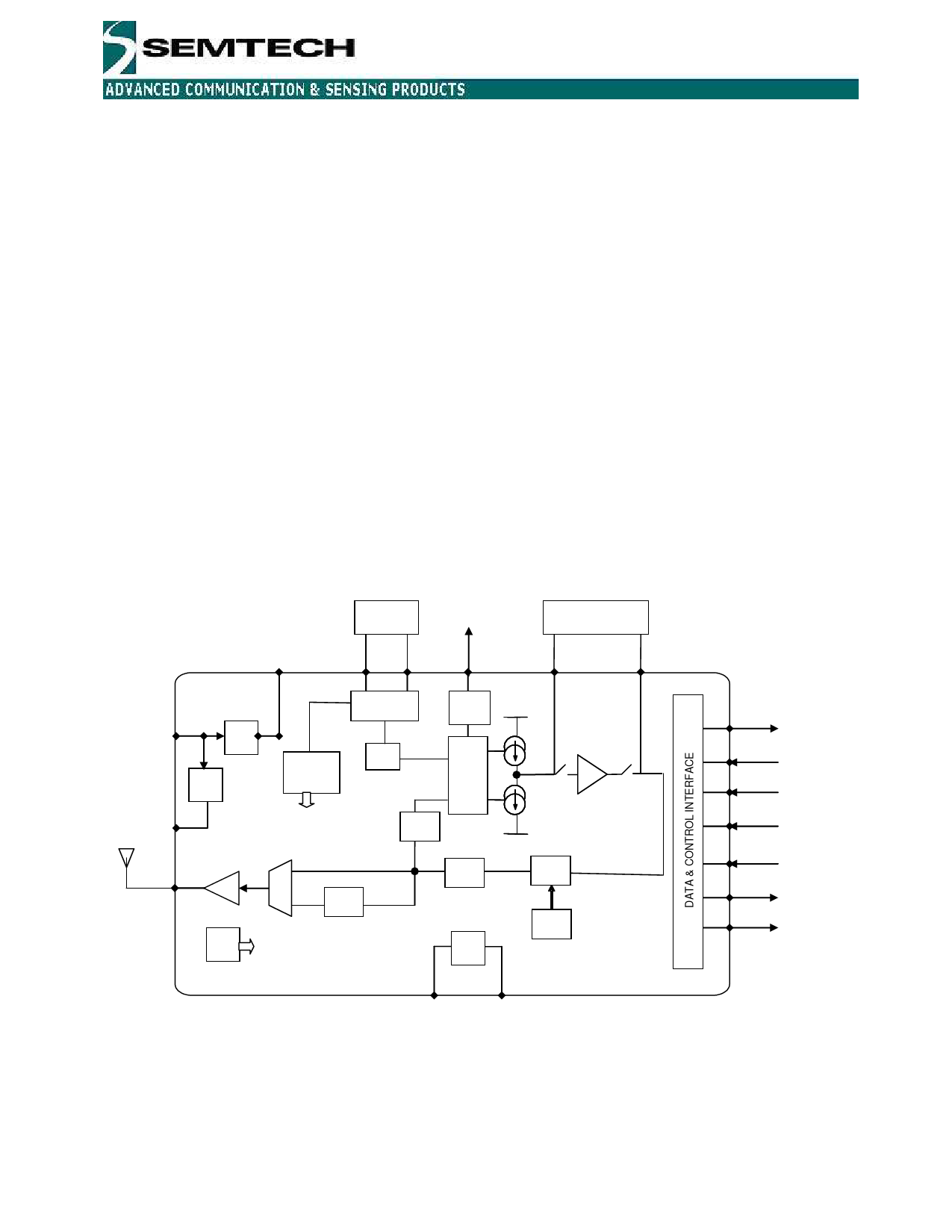
1 FUNCTIONAL BLOCK DIAGRAM
CRYSTAL
LOOP FILTER
VDDF
XTA XTB
LD
CPOUT
VARIN
VDD
LDO
LDO
VDDP
RFOUT
PA
BIAS
OSCILLATOR
LOCK
DETECT
CLOCK
GEN
÷M
PPFFDD
÷ NN,,AA
Open Loop
OPAMP
÷ 22
VVCCO O
÷ 22
MOD
LDO
SX1223
VDDD
VDD
Figure 1: SX1223 block diagram
SO
SI
EN
SCK
DATAIN
DCLK
CLKOUT
© Semtech 2007
www.semtech.com
3
Share Link: 