T35L6432B 데이터 시트보기 (PDF) - Taiwan Memory Technology
부품명
상세내역
제조사
T35L6432B Datasheet PDF : 16 Pages
| |||
tm TE
CH
T35L6432B
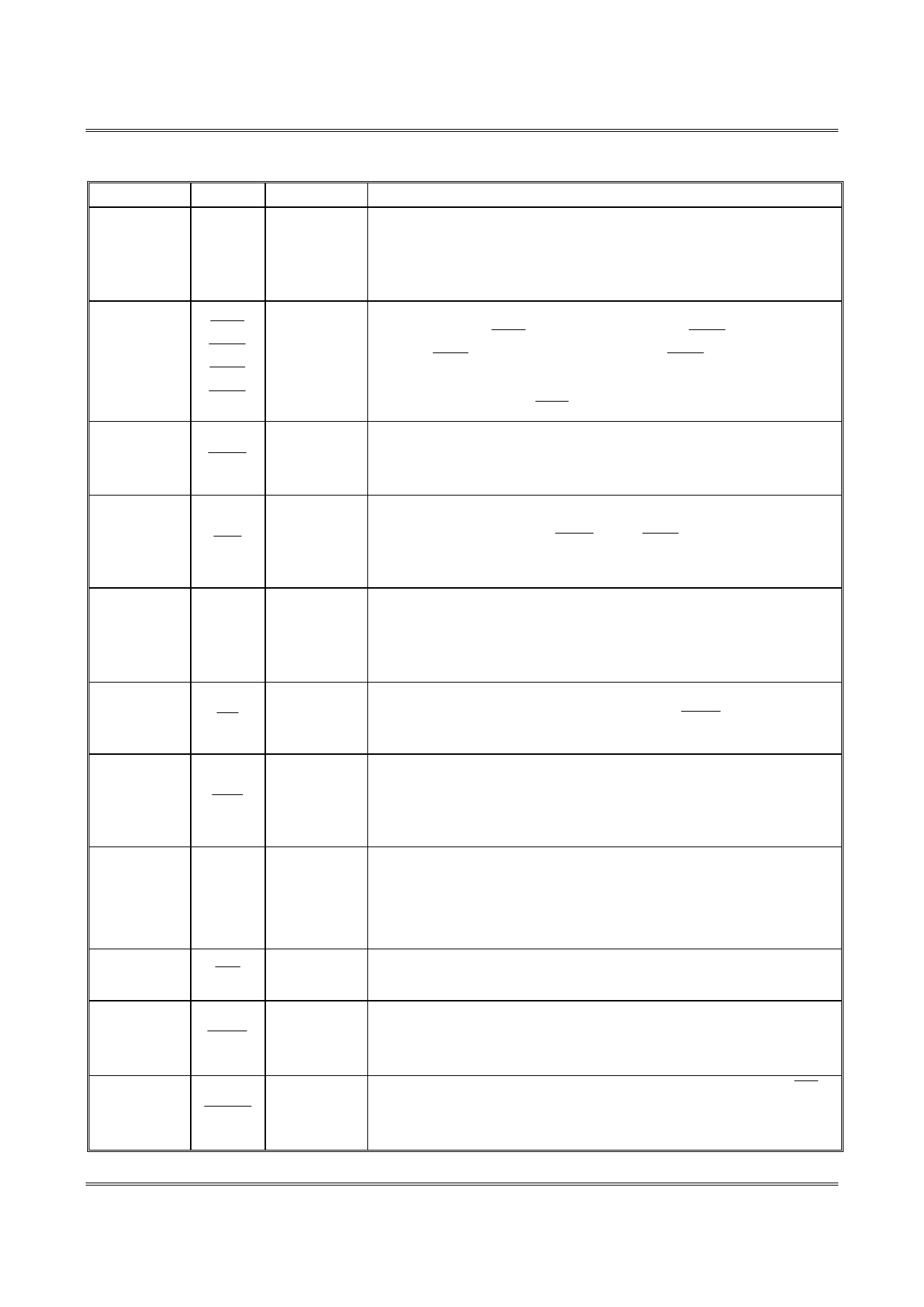
PIN DESCRIPTIONS
PINS
SYM. TYPE
DESCRIPTION
32-37, 44-49,
81, 82, 99,
100,
A0-A15
Addresses: These inputs are registered and must meet the setup and
Input- hold times around the rising edge of CLK. The burst counter
Synchronous generates internal addresses associated with A0 and A1, during
burst cycle and wait cycle.
93-96
BW1
BW2
BW3
BW4
Byte Writes: A byte write is LOW for a WRITE cyle and HIGH for
a READ cycle. BW1 controls DQ1-DQ8. BW2 controls DQ9-
Input-
DQ16. BW3 controls DQ17-DQ24. BW4 controls DQ25-
Synchronous
DQ32. Data I/O are high impedance if either of these inputs are
LOW , conditioned by BWE being LOW.
Write Enable: This active LOW input gates byte write operations
Input-
87
BWE
and must meet the setup and hold times around the rising edge of
Synchronous
CLK.
Global Write: This active LOW input allows a full 32-bit WRITE to
Input-
88
GW
occur independent of the BWE and BWn lines and must meet
Synchronous
the setup and hold times around the rising edge of CLK.
Clock: This signal registers the addresses, data, chip enables,
Input- writecontrol and burst control inputs on its rising edge. All
89
CLK
Synchronous synchronous inputs must meet setup and hold times around the
clock's rising edge.
Synchronous Chip Enable: This active LOW input is used to enable
Input-
98
CE
the device and conditions internal use of ADSP. This input is
Synchronous
sampled only when a new external address is loaded.
Synchronous Chip Enable: This active LOW input is used to enable
Input-
92
CE2
the device. This input is sampled only when a new external address
Synchronous
is loaded. This input can be used for memory depth expansion.
Synchronous Chip Enable: This active HIGH input is used to enable
97
CE2
Input- the device. This input is sampled only when a new external address
Synchronous
is loaded. This input can be used for memory depth expansion.
Output enable: This active LOW asynchronous input enables the
86
OE
Input
data output drivers.
Input- Address Advance: This active LOW input is used to control the
83
ADV
internal burst counter. A HIGH on this pin generates wait cycle
Synchronous
(no address advance).
Address Status Processor: This active LOW input, along withCE
Input-
84
ADSP Synchronous being LOW, causes a new external address to be registered and a
READ cycle is initiated using the new address.
Taiwan Memory Technology, Inc. reserves the right P. 4
to change products or specifications without notice.
Publication Date: JUL. 2002
Revision: A
Share Link: 