TA7368PG 데이터 시트보기 (PDF) - Toshiba
부품명
상세내역
제조사
TA7368PG Datasheet PDF : 12 Pages
| |||
TA7368PG/FG
Precaution For Use And Application
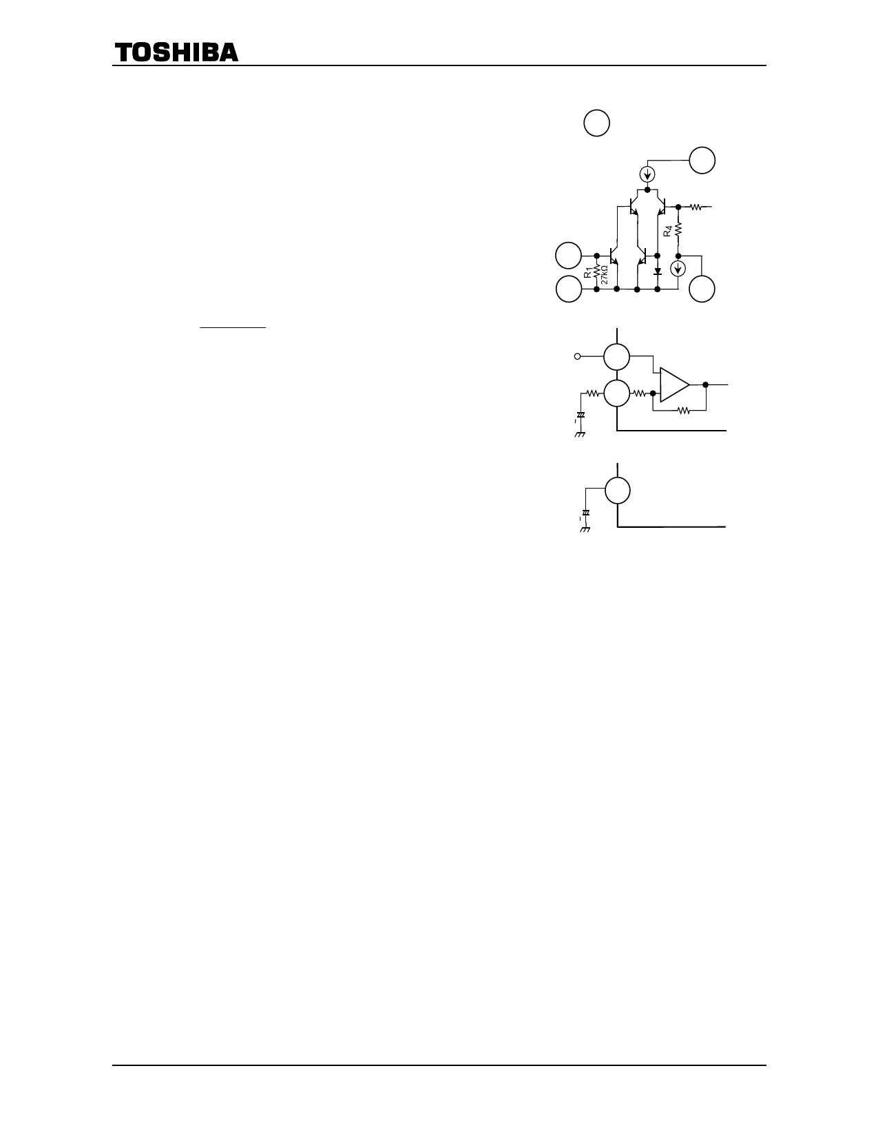
1. Input stage
The input stage of power amplifier (equivalent circuit) is comprised of a
PNP differential pair (Q2 and Q3) preceded by a PNP emitter follower
(Q1) which allows DC referencing of the source signal to ground. This
eliminated the need for an input coupling capacitor. However, in case the
brush noise of volume becomes a problem, provide serially a coupling
capacitor to the input side.
/ : TA7368PG / TA7368FG
9/2
Q2 Q3
FROM PIN 7 / 10
R5
2. Adjustment of voltage gain
The voltage gain is fixed at GV≒40dB by the resistors (R4 and R5) in IC,
however, its reduction is possible through adding Rf as shown in Figure 2.
In this case, the voltage gain is obtained by the following equation.
GV
=
20log
R5 + R4 +
R4 + Rf
Rf
It is recommended to use this IC with the voltage gain of GV = 28dB or
over.
3. Ripple rejection ratio
Adding CRIP, to ripple terminal 2 as shown in Figure 3, the ripple
rejection ratio is improved from −25dΒ typ. to −45dΒ typ.
1/4
Q1 Q4
5/8
D1
3/6
Fig.1
IN
Vin
1/4
NF
Rf
R4
3/6
+
90Ω
+
− R5
10Ω
Fig.2
4. Power dissipation
Care should be taken to use this IC below maximum power dissipation.
Because it may over absolute maximum rating depending on operating
condition.
• TA7368PG PD = 900mW (Ta = 25°C)
• TA7368FG PD = 400mW (Ta = 25°C)
RIPPLE
2/5
CRIP +
Fig.3
5. Phase−compensation
Small temperature coefficient and excellent frequency characteristic is needed by capacitors below.
• Oscillation preventing capacitors for power amplifier output
• Bypass capacitor for ripple filter
• Capacitor between VCC and GND
2
2006-04-28
Share Link: 