TA8061 데이터 시트보기 (PDF) - Toshiba
부품명
상세내역
제조사
TA8061 Datasheet PDF : 6 Pages
| |||
TA8061H
PIN DESCRIPTION
PIN No.
1, 12
2, 11
3, 10
SYMBOL
VCC
OUT
DIAG
DESCRIPTION
Power supply pin. A function for protection against over-voltage is provided so that the output
will turn off when the applied voltage exceeds 27.5V (Typ.).
This function works to protect the IC and load.
PNP-type complementary output pin with a current capacity of 1.5A. When the output pin is
supplied with a current exceeding the detection current (typically 3A) because of load
short-circuit, the output is latched to the OFF state to protect the IC. To restart, turn off the input
once, then raise it high.
Self-diagnosis detection pin. This signal goes low when the output is short-circuited or opened
while the input is on (high). The output will be latched when the load is short-circuited, but will
not when the load is opened. This pin supplies an NPN open-collector output.
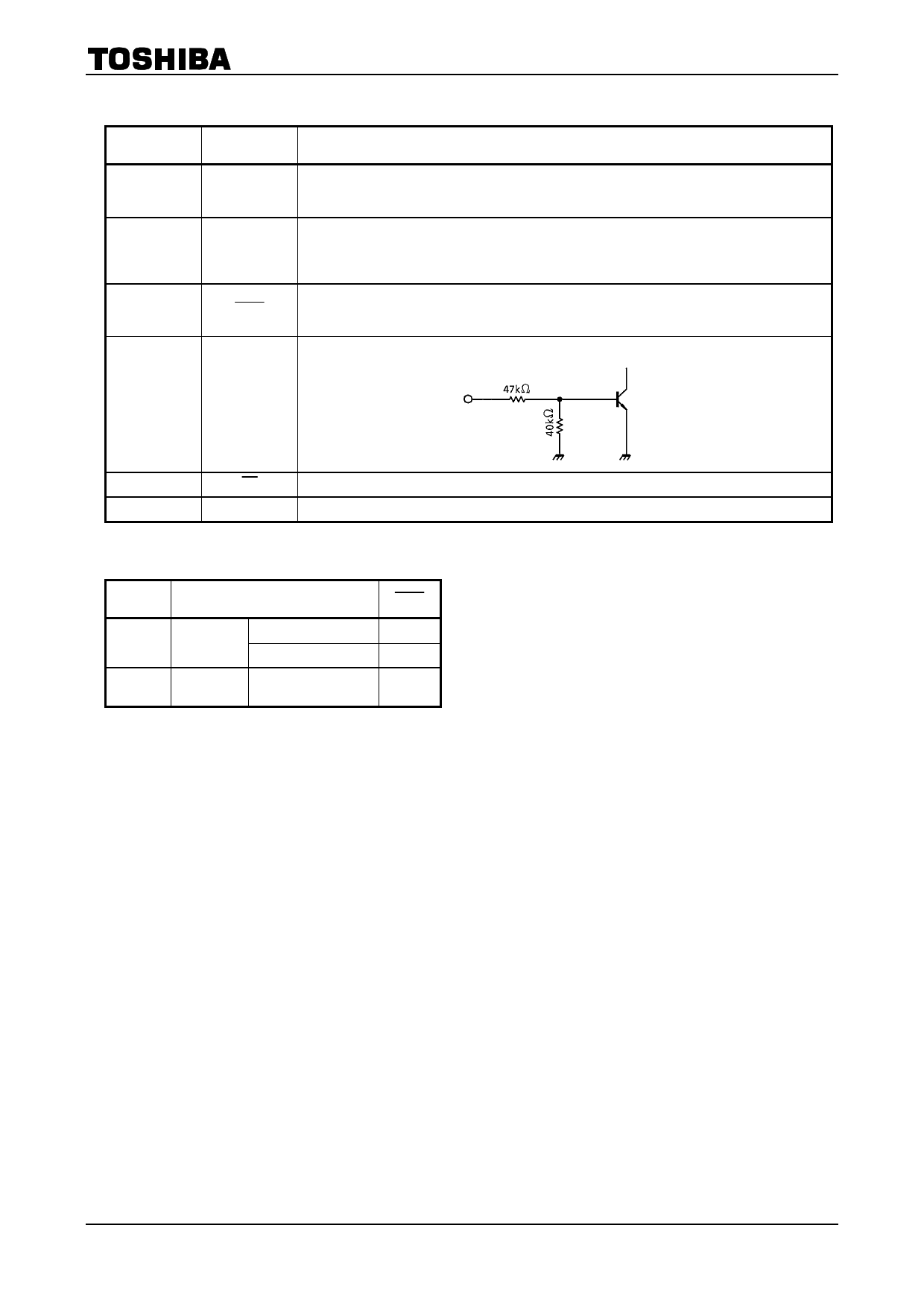
TTL-compatible input pin. The circuit is shown as follows.
4, 9
IN
5, 8
EN
When this signal goes high, both channels 1 and 2 are placed in standby state (0.5mA Max.).
6, 7
GND
Grounded.
TRUTH TABLE
IN
OUT
H
H
(ON)
Normal
Abnormal
L
L
(OFF)
―
DIAG
H
L
H
2
2002-02-27
Share Link: 