TA8182 데이터 시트보기 (PDF) - Toshiba
부품명
상세내역
제조사
TA8182 Datasheet PDF : 11 Pages
| |||
TA8182FN
Application Note
1. PW SW
It is necessary to connect an external pull-down resistor with the terminal PW SW (pin(7)), in case that this
IC is turned on due to external noise etc.
2. MODE SW
It is necessary to connect an external pull-down resistor with the terminal MODE SW (pin(6)), in case that
this IC doesn’t operate normally due to external noise etc.
3. RF GND
This IC has two GND terminals (pin(3): RF GND, pin(16): GND). External parts shown in below should be
connected with RF GND (pin(3)), and other parts should be connected with GND (pin(16)).
· By-pass capacitor at pin(14) (FM RF) and pin(15) (TV RF)
· By-pass capacitor at pin(4) (FM BY) and pin(2) (TV BY)
The pattern diagram of capacitor connected with pin(2) and pin(4) should be shortly, because RF circuit and
MIX circuit operate on the voltage of pin(2) or pin(4).
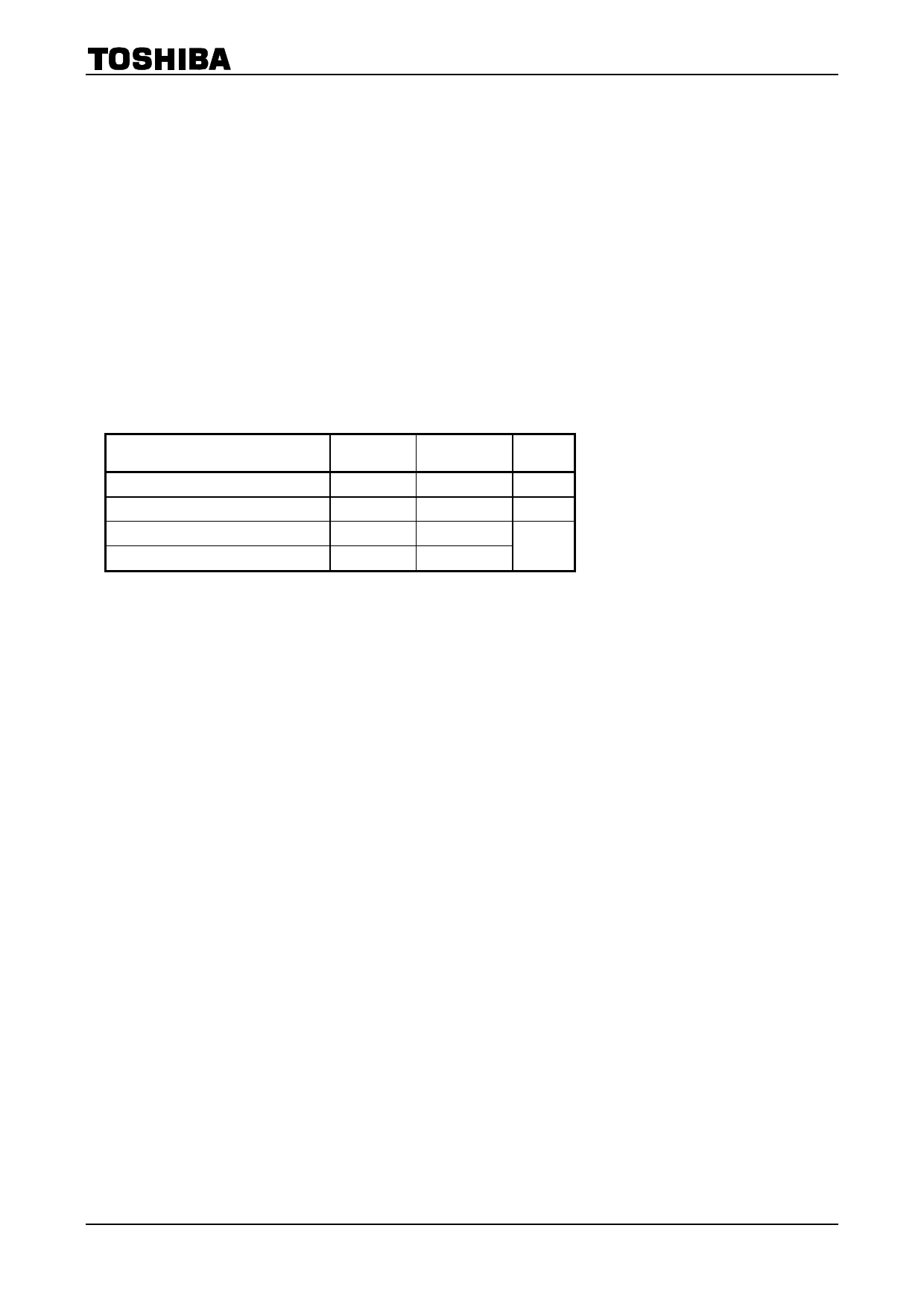
Maximum Ratings (Ta = 25°C)
Characteristic
Symbol
Rating
Unit
Supply voltage
Power dissipation
(Note)
Operating temperature
Storage temperature
VCC
4.5
V
PD
400
mW
Topr
-25~75
°C
Tstg
-55~150
(Note) Derated above Ta = 25°C in the proportion of 3.2mW / °C.
4
2002-10-30
Share Link: 