TA8220HQ 데이터 시트보기 (PDF) - Toshiba
부품명
상세내역
제조사
TA8220HQ Datasheet PDF : 15 Pages
| |||
TA8220HQ
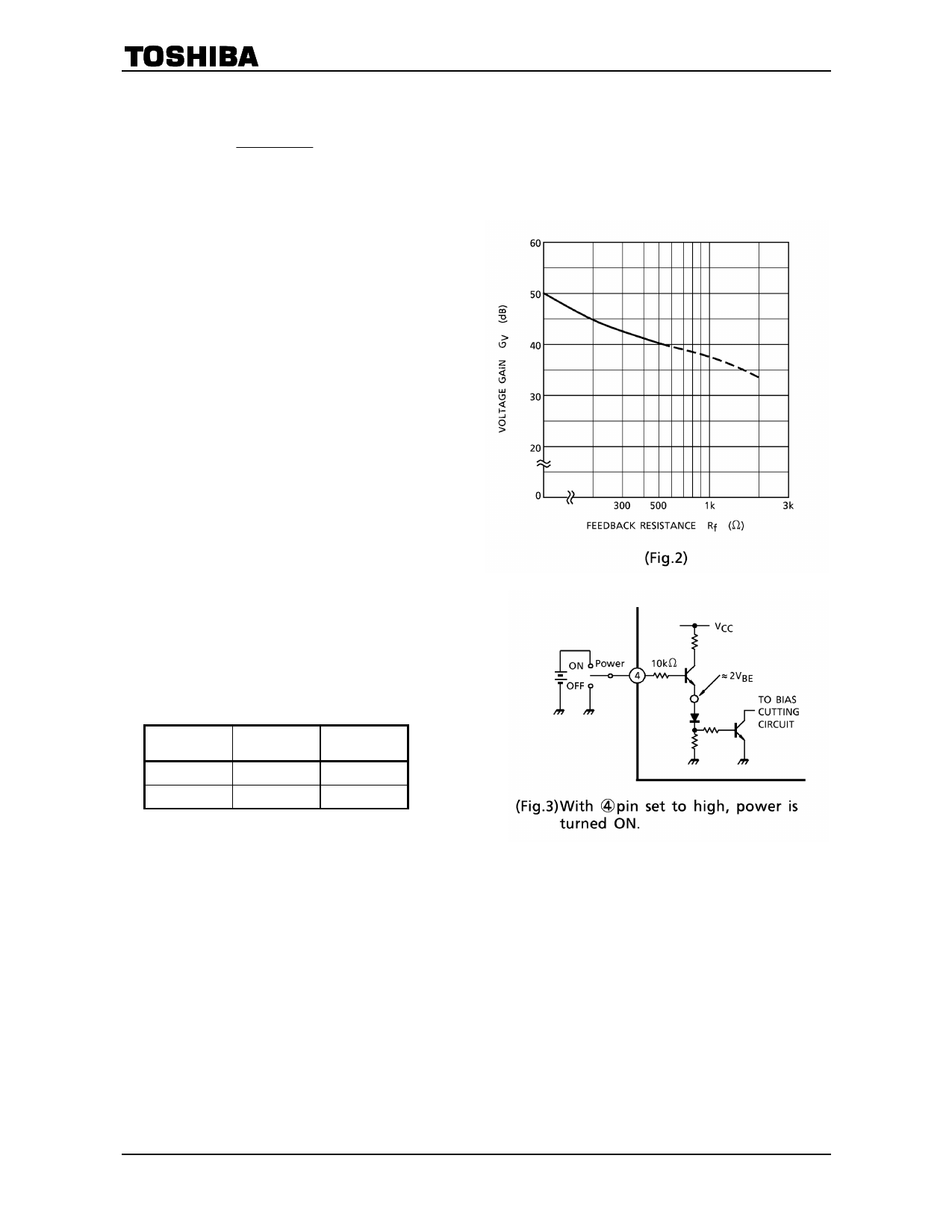
The total closed loop gain GV of this IC can be obtained by expression below when the closed loop voltage gain of
amp1 is GV1.
GV1
=
20log
R1
+ (Rf + R2
Rf + R2
)
(dB)LLL (1)
The closed loop voltage gain of power amp, amp3 and amp4 is fixed at GV3≒GV4 = 20dB.
Therefore, the total closed circuit voltage gain GV is obtained through BTL connection by the expression below.
GV = GV1 + GV3 + 6 (dB)………(2)
For example, when Rf = 0Ω, GV is obtained by the
expressions (1) and (2) as shown below.
GV≒24 + 20 + 6 = 50dB
The voltage gain is reduced when Rf is increased.
(Fig.2)
With the voltage gain reduced, since (1) the
oscillation stability is reduced, and (2) the pop noise
changes when VCC is set to on, refer to the items 3
and 4.
2. Stand−by SW function
By means of controlling (4)pin (stand−by terminal) to
high and low, the power supply can be set to on and off.
The threshold voltage of (4)pin is set at 2.1V (3VBE), and
the power supply current is about 1µA (typ.) at the
stand−by state.
Control voltage of (4)pin: V (SB)
Stand−By
Power
V (SB) (V)
On
Off
0~2
Off
On
3~VCC
<Adjustage of stand−by SW>
(1) Since VCC can directly be controlled to on / off by the microcomputer, the switching relay can be omitted.
(2) Since the control current is microscopic, the switching relay of small current capacity is satisfactory for
switching.
3
2006-04-28
Share Link: 