TC1073-28VCH 데이터 시트보기 (PDF) - Microchip Technology
부품명
상세내역
제조사
TC1073-28VCH
Microchip Technology

TC1073-28VCH Datasheet PDF : 20 Pages
| |||
TC1072/TC1073
3.0 DETAILED DESCRIPTION
The TC1072 and TC1073 are precision fixed output
voltage regulators. (If an adjustable version is desired,
please see the TC1070/TC1071/TC1187 data sheet.)
Unlike bipolar regulators, the TC1072 and TC1073’s
supply current does not increase with load current. In
addition, VOUT remains stable and within regulation
over the entire 0mA to IOUTMAX load current range, (an
important consideration in RTC and CMOS RAM
battery back-up applications).
Figure 3-1 shows a typical application circuit. The
regulator is enabled any time the shutdown input
(SHDN) is at or above VIH, and shutdown (disabled)
when SHDN is at or below VIL. SHDN may be
controlled by a CMOS logic gate, or I/O port of a
microcontroller. If the SHDN input is not required, it
should be connected directly to the input supply. While
in shutdown, supply current decreases to 0.05µA
(typical), VOUT falls to zero volts, and ERROR is open-
circuited.
FIGURE 3-1:
TYPICAL APPLICATION
CIRCUIT
+
1µF
+
Battery
VIN
VOUT
TC1072
TC1073
GND
Bypass
VOUT
+
1µF
C1
C3, 470pF
Shutdown Control
(to CMOS Logic or Tie
to VIN if unused)
SHDN ERROR
C2 Required Only
if ERROR is used as a
Processor RESET Signal
(See Text)
V+
R1
1M
0.2µF
C2
BATTLOW
or RESET
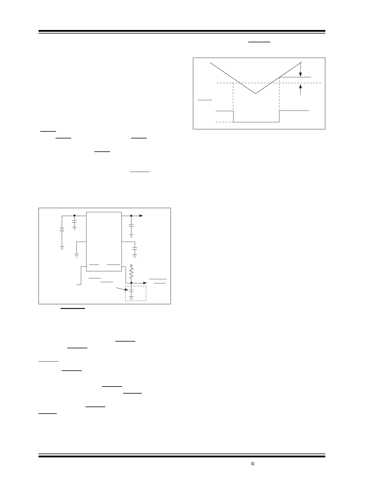
3.1 ERROR Open Drain Output
ERROR is driven low whenever VOUT falls out of
regulation by more than – 5% (typical). This condition
may be caused by low input voltage, output current
limiting, or thermal limiting. The ERROR output voltage
value (e.g. ERROR = VOL at 4.75V (typ.) for a 5.0V
regulator and 2.85V (typ.) for a 3.0V regulator).
ERROR output operation is shown in Figure 3-2.
Note that ERROR is active when VOUT falls to VTH, and
inactive when VOUT rises above VTH by VHYS.
As shown in Figure 3-1, ERROR can be used as a
battery low flag, or as a processor RESET signal (with
the addition of timing capacitor C2). R1 x C2 should be
chosen to maintain ERROR below VIH of the processor
RESET input for at least 200 msec to allow time for the
system to stabilize. Pull-up resistor R1 can be tied to
VOUT, VIN or any other voltage less than (VIN + 0.3V).
FIGURE 3-2:
VOUT
VTH
ERROR OUTPUT
OPERATION
HYSTERESIS (VH)
ERROR
VIH
VOL
3.2 Output Capacitor
A 1µF (min) capacitor from VOUT to ground is
recommended. The output capacitor should have an
effective series resistance greater than 0.1Ω and less
than 5.0Ω, and a resonant frequency above 1MHz. A
1µF capacitor should be connected from VIN to GND if
there is more than 10 inches of wire between the
regulator and the AC filter capacitor, or if a battery is
used as the power source. Aluminum electrolytic or
tantalum capacitor types can be used. (Since many
aluminum electrolytic capacitors freeze at approxi-
mately -30°C, solid tantalums are recommended for
applications operating below -25°C.) When operating
from sources other than batteries, supply-noise
rejection and transient response can be improved by
increasing the value of the input and output capacitors
and employing passive filtering techniques.
3.3 Bypass Input
A 470pF capacitor connected from the Bypass input to
ground reduces noise present on the internal
reference, which in turn significantly reduces output
noise. If output noise is not a concern, this input may be
left unconnected. Larger capacitor values may be
used, but results in a longer time period to rated output
voltage when power is initially applied.
DS21354B-page 6
© 2002 Microchip Technology Inc.
Share Link: