TC1073-28VCH 데이터 시트보기 (PDF) - Microchip Technology
부품명
상세내역
제조사
TC1073-28VCH
Microchip Technology

TC1073-28VCH Datasheet PDF : 20 Pages
| |||
4.0 THERMAL CONSIDERATIONS
4.1 Thermal Shutdown
Integrated thermal protection circuitry shuts the
regulator off when die temperature exceeds 160°C.
The regulator remains off until the die temperature
drops to approximately 150°C.
4.2 Power Dissipation
The amount of power the regulator dissipates is
primarily a function of input and output voltage, and
output current. The following equation is used to
calculate worst case actual power dissipation:
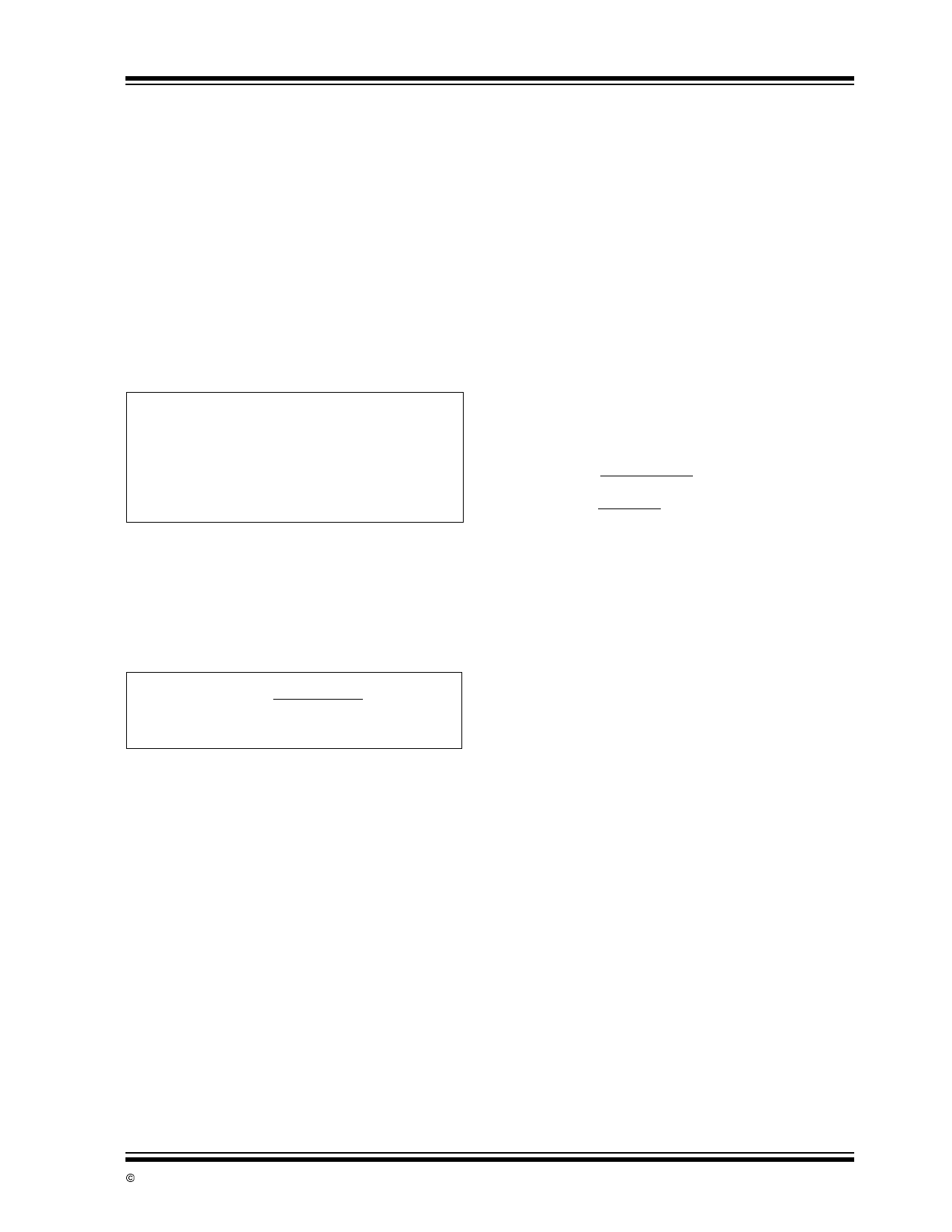
EQUATION 4-1:
PD ≈ (VINMAX – VOUTMIN)ILOADMAX
Where:
PD = Worst case actual power dissipation
VINMAX = Maximum voltage on VIN
VOUTMIN = Minimum regulator output voltage
ILOADMAX = Maximum output (load) current
The maximum allowable power dissipation (Equation
4-2) is a function of the maximum ambient temperature
(TAMAX), the maximum allowable die temperature
(TJMAX) and the thermal resistance from junction-to-air
(θJA). The 6-Pin SOT-23A package has a θJA of
approximately 220°C/Watt.
EQUATION 4-2:
PDMAX= (TJMAX – TAMAX)
θJA
Where all terms are previously defined.
TC1072/TC1073
Equation 4-1 can be used in conjunction with Equation
4-2 to ensure regulator thermal operation is within
limits. For example:
Given:
VINMAX = 3.0V ±5%
VOUTMIN = 2.7V – 2.5%
ILOADMAX = 40mA
TJMAX = 125°C
TAMAX = 55°C
Find: 1. Actual power dissipation
2. Maximum allowable dissipation
Actual power dissipation:
PD ≈ (VINMAX – VOUTMIN)ILOADMAX
= [(3.0 x 1.05) – (2.7 x .975)]40 x 10–3
= 20.7mW
Maximum allowable power dissipation:
PDMAX = (TJMAX – TAMAX)
θJA
= (125 – 55)
220
= 318mW
In this example, the TC1072 dissipates a maximum of
20.7mW; below the allowable limit of 318mW. In a
similar manner, Equation 4-1 and Equation 4-2 can be
used to calculate maximum current and/or input
voltage limits.
4.3 Layout Considerations
The primary path of heat conduction out of the package
is via the package leads. Therefore, layouts having a
ground plane, wide traces at the pads, and wide power
supply bus lines combine to lower θJA and therefore
increase the maximum allowable power dissipation
limit.
© 2002 Microchip Technology Inc.
DS21354B-page 7
Share Link: