TC913A 데이터 시트보기 (PDF) - Microchip Technology
부품명
상세내역
제조사
TC913A Datasheet PDF : 12 Pages
| |||
1.0 ELECTRICAL
CHARACTERISTICS
Absolute Maximum Ratings*
Total Supply Voltage (VDD to VSS) ....................... +18V
Input Voltage ...................... (VDD +0.3V) to (VSS -0.3V)
Current Into Any Pin........................................... 10 mA
While Operating ......................................... 100 μA
Package Power Dissipation (TA – 70°C)
Plastic DIP ............................................... 730 mW
Plastic SOIC ............................................ 470 mW
Operating Temperature Range
C Device .......................................... 0°C to +70°C
Storage Temperature Range.............. -65°C to +150°C
TC913A/TC913B
*Stresses above those listed under “Absolute
Maximum Ratings” may cause permanent damage to
the device. These are stress ratings only and functional
operation of the device at these or any other conditions
above those indicated in the operation sections of the
specifications is not implied. Exposure to Absolute
Maximum Rating conditions for extended periods may
affect device reliability.
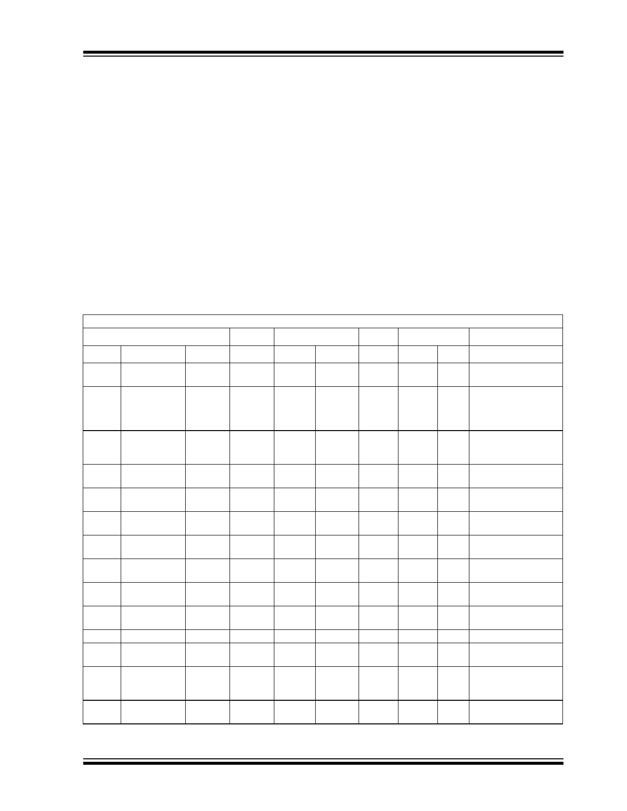
TC913A AND TC913B ELECTRICAL SPECIFICATIONS
Electrical Characteristics: VS = ±5V, TA = +25°C, unless otherwise indicated.
TC913A
TC913B
Symbol Parameter
Min
Typ
VOS Input Offset
—
5
Voltage
TCVOS Average Temp.
—
0.05
Coefficient of
—
0.05
Input Offset
Voltage
IB Average Input
—
—
Bias Current
—
—
—
—
IOS Average Input
—
5
Offset Current
—
—
eN Input Voltage
—
0.6
Noise
—
11
CMRR Common Mode 110
116
Rejection Ratio
CMVR Common Mode
VSS
—
Voltage Range
AOL Open-Loop
115
120
Voltage Gain
VOUT Output Voltage VSS + 0.3
—
Swing
BW Closed Loop
—
1.5
Bandwidth
SR Slew Rate
—
2.5
PSRR Power Supply
110
—
Rejection Ratio
VS Operating
±3.5
—
Supply Voltage
7.0
—
Range
IS Quiescent
—
0.65
Supply Current
Note 1: Characterized; not 100% tested.
Max
Min
15
—
0.15
—
0.15
—
90
—
3
—
4
—
20
—
1
—
—
—
—
—
—
100
VDD - 2
VSS
—
110
VDD - 0.9 VSS + 0.3
—
—
—
—
—
100
±8.3
±3.5
16
7.0
0.85
—
Typ
Max Unit
Test Conditions
15
30
μV TA = +25°C
0.1
0.25 μV/°C 0°C ≤ TA ≤ +70°C
0.1
0.25 μV/°C -25°C ≤ TA ≤ +85°C
(Note 1)
—
120
pA TA = +25°C
—
4
nA 0°C ≤ TA ≤ +70°C
—
6
nA -25°C ≤ TA ≤ +85°
10
40
pA TA = +25°C
—
1
nA TA = +85°C
0.6
—
μVP-P 0.1 to 1 Hz, RS ≤ 100Ω
11
—
μVP-P 0.1 to 10 Hz, RS ≤ 100Ω
110
—
dB VSS ≤ VCM ≤ VDD - 2.2
—
VDD - 2
V
120
—
dB RL = 10 kΩ, VOUT = ±4V
—
VDD -0.9 V RL = 10 kΩ
1.5
—
MHz Closed Loop Gain = +1
2.5
— V/μsec RL = 10 kΩ, CL = 50 pF
—
—
dB ±3.3V to ±5.5V
—
±8.3
V Split Supply
—
16
V Single Supply
—
1.1
mA VS = ±5V
© 2006 Microchip Technology Inc.
DS21482C-page 3
Share Link: 