TCD1305 데이터 시트보기 (PDF) - Toshiba
부품명
상세내역
제조사
TCD1305 Datasheet PDF : 14 Pages
| |||
TCD1305P
OPTICAL / ELECTRICAL CHARACTERISTICS
(Ta=25°C, Vφ=5.0V (PULSE), f φ=0.5MHz, tINT (INTEGRATION TIME)=10ms,
LOAD RESISTANCE=100kΩ, VAD=VDD=5.0V,
LIGHT SOURCE=DAYLIGHT FLUORESCENT LAMP)
CHARACTERISTIC
SYMBOL
MIN. TYP. MAX. UNIT
NOTE
Sensitivity
Photo Response Non Uniformity
Register Imbalance
Saturation Output Voltage
Dark Signal Voltage
Total Transfer Effeiciency
Dynamic Range
Saturation Exposure
DC Power Dissipation
DC Signal Output Voltage
Output Impedance
Image Lag of Electronic Shutter
R
PRNU
RI
VSAT
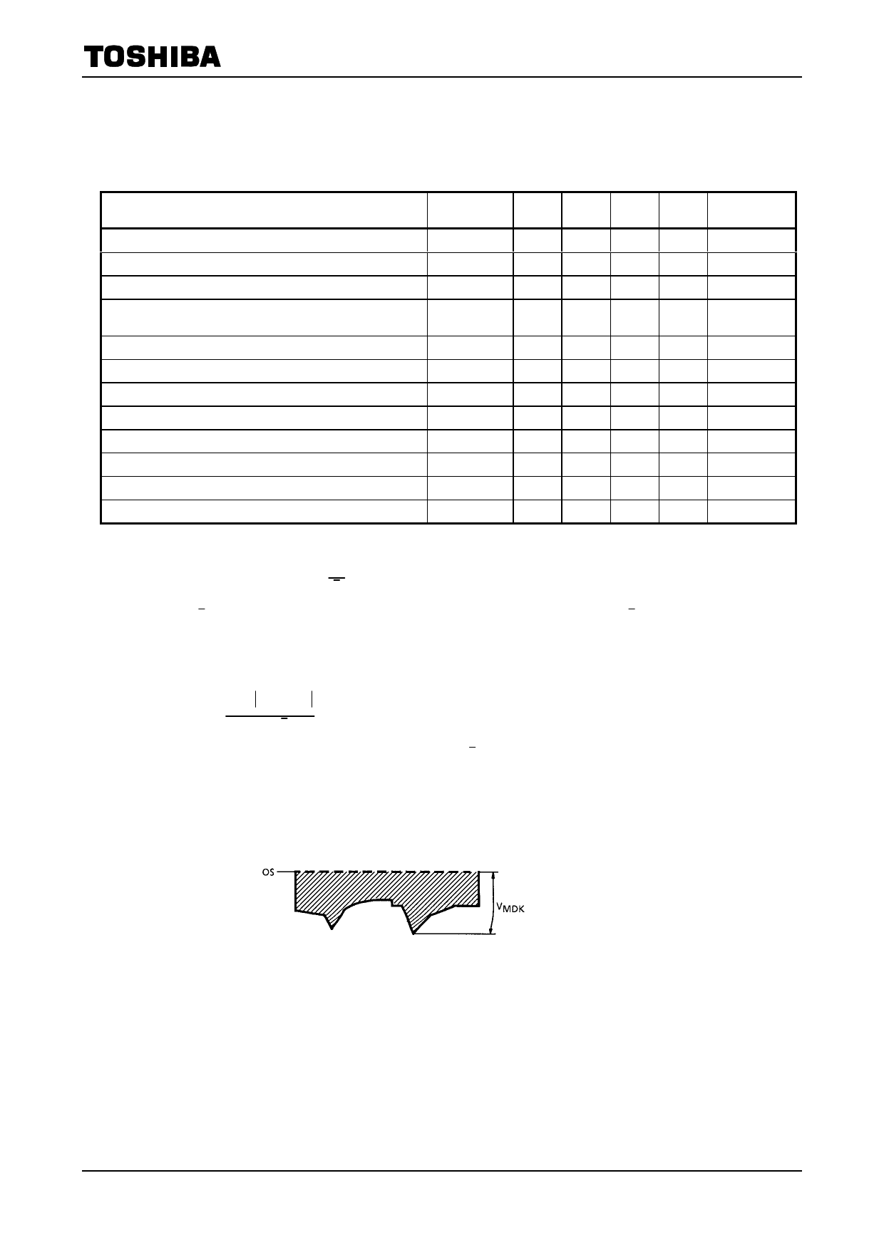
VMDK
TTE
DR
SE
PD
VOS
Zo
VLAGICG
44.8
64
―
―
―
―
1.2
―
―
2
92
95
―
300
― 0.004
―
25
1.7
2.5
―
0.5
―
―
― V / lx·s
10
%
(Note 2)
3
%
(Note 3)
―
V
VOD=4.5V
(Note 4)
5
mV
(Note 5)
―
%
―
―
(Note 6)
―
lx·s
(Note 7)
75
mW
3.5
V
(Note 8)
1.0
kΩ
10
mV
Tint=100µs
Note 2: Measured at 50% of SE (Typ.)
Definition of PRNU: PRNU= Dc ´100
%
c
Where ? is average of total signal outputs and ,? is the maximum deviation from ? under uniform illumination.
Note 3: Measured at 50% of SE (Typ.)
RI is defined as follows:
3647
å cn - cn + 1
RI = n=1
´ 100
%
3647·c
Where ? n and ? n+1 are signal outputs of each pixel. ? is average of total signal outputs.
Note 4: VSAT is defined as minimum saturation output voltage of all effective pixels.
Note 5: VMDK is defined as maximum dark signal voltage of all effective pixels.
3
2001-10-15
Share Link: 