M80C186 데이터 시트보기 (PDF) - Intel
부품명
상세내역
제조사
M80C186 Datasheet PDF : 59 Pages
| |||
M80C186
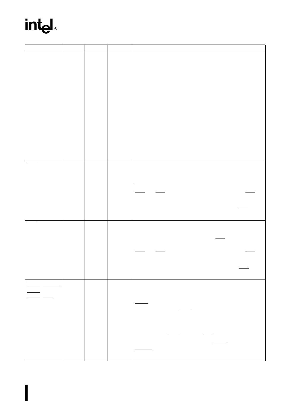
Symbol
HOLD (input)
HLDA (output)
PGA
50
51
UCS
34
LCS
33
MCS0 PEREQ 38
MCS1 ERROR 37
MCS2
36
MCS3 NPS
35
Table 1 M80C186 Pin Description (Continued)
QFP
28
27
44
45
40
41
42
43
Type
I
O
O
O
IO
IO
O
O
Name and Function
HOLD indicates that another bus master is requesting the
local bus The HOLD input is active HIGH HOLD may be
asynchronous with respect to the M80C186 clock The
M80C186 will issue a HLDA (HIGH) in response to a HOLD
request at the end of T4 or Ti Simultaneous with the
issuance of HLDA the M80C186 will float the local bus and
control lines After HOLD is detected as being LOW the
M80C186 will lower HLDA When the M80C186 needs to
run another bus cycle it will again drive the local bus and
control lines
In Enhanced Mode HLDA will go low when a DRAM
refresh cycle is pending in the M80C186 and an external
bus master has control of the bus It will be up to the
external master to relinquish the bus by lowering HOLD so
that the M80C186 may execute the refresh cycle Lowering
HOLD for four clocks and returning HIGH will insure only
one refresh cycle to the external master HLDA will
immediately go active after the refresh cycle has taken
place
Upper Memory Chip Select is an active LOW output
whenever a memory reference is made to the defined
upper portion (1K – 256K block) of memory This line is not
floated during bus HOLD The address range activating
UCS is software programmable
UCS and LCS are sampled upon the rising edge of RES If
both pins are held low the M80C186 will enter ONCE
Mode In ONCE Mode all pins assume a high impedance
state and remain so until a subsequent RESET UCS has a
weak internal pullup for normal operation
Lower Memory Chip Select is active LOW whenever a
memory reference is made to the defined lower portion
(1K – 256K) of memory This line is not floated during bus
HOLD The address range activating LCS is software
programmable
UCS and LCS are sampled upon the rising edge of RES If
both pins are held low the M80C186 will enter ONCE
Mode In ONCE Mode all pins assume a high impedance
state and remain so until a subsequent RESET UCS has a
weak internal pullup for normal operation
Mid-Range Memory Chip Select signals are active LOW
when a memory reference is made to the defined mid-
range portion of memory (8K – 512K) These lines are not
floated during bus HOLD The address ranges activating
MCS0 – 3 are software programmable
In Enhanced Mode MCS0 becomes a PEREQ input
(Processor Extension Request) When connected to the
Numerics Processor Extension this input is used to signal
the M80C186 when to make numeric data transfers to and
from the NPX MCS3 becomes NPS (Numeric Processor
Select) which may only be activated by communication to
the Numerics Processor Extension MCS1 becomes
ERROR in enhanced mode and is used to signal numerics
coprocessor errors
7
Share Link: 