TDA1543 데이터 시트보기 (PDF) - Philips Electronics
부품명
상세내역
제조사
TDA1543 Datasheet PDF : 13 Pages
| |||
Philips Semiconductors
Dual 16-bit DAC (economy version)
(I2S input format)
Product specification
TDA1543
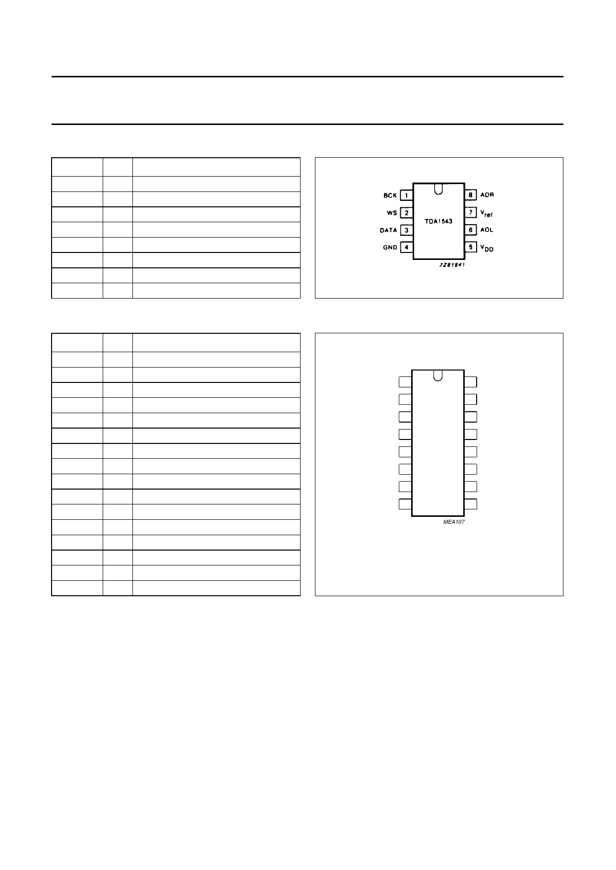
PINNING
SYMBOL PIN
DESCRIPTION
BCK
1 bit clock input
WS
2 word select input
DATA
3 data input
GND
VDD
AOL
4 ground
5 +5 V supply voltage
6 left channel voltage output
Vref
AOR
7 reference voltage output
8 right channel output
Fig.2 Pin configuration TDA1543.
PINNING
SYMBOL PIN DESCRIPTION
n.c.
1 not connected
n.c.
2 not connected
BCK
3 bit clock input
WS
4 word select input
DATA
5 data input
GND
6 ground
n.c.
7 not connected
n.c.
8 not connected
n.c.
9 not connected
n.c.
VDD
AOL
10 not connected
11 +5 V supply voltage
12 left channel output
Vref
AOR
13 reference voltage output
14 right channel output
n.c.
15 not connected
n.c.
16 not connected
handbook, halfpage
n.c. 1
16 n.c.
n.c. 2
15 n.c.
BCK 3
14 AOR
WS 4
13 Vref
TDA1543T
DATA 5
12 AOL
GND 6
n.c. 7
11 VDD
10 n.c.
n.c. 8
9 n.c.
MEA107
Fig.3 Pin configuration TDA1543T.
February 1991
4
Share Link: 