TDA4867 데이터 시트보기 (PDF) - Philips Electronics
부품명
상세내역
제조사
TDA4867 Datasheet PDF : 14 Pages
| |||
Philips Semiconductors
Full bridge current driven vertical
deflection booster
Preliminary specification
TDA4867J
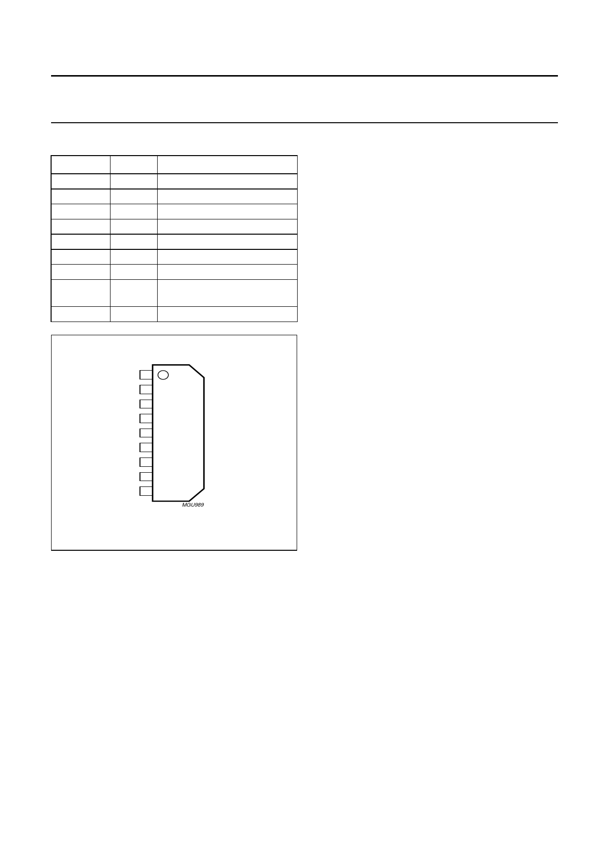
PINNING
SYMBOL
INP
INN
VP
OUTB
GND
OUTA
VFB
GUARD
FEEDB
PIN
DESCRIPTION
1 non-inverted input
2 inverted input
3 supply voltage
4 output B
5 ground
6 output A
7 flyback supply voltage
8 guard output or power save
mode input
9 feedback input
handbook, halfpage
INP 1
INN 2
VP 3
OUTB 4
GND 5 TDA4867J
OUTA 6
VFB 7
GUARD 8
FEEDB 9
MGU989
Fig.2 Pin configuration.
FUNCTIONAL DESCRIPTION
The TDA4867J consists of a differential input stage, two
output stages, a flyback generator, a protection circuit for
the output stages and a guard circuit.
Differential input stage
The differential input stage has a high CMRR differential
current mode input (pin INP and pin INN) that results in a
high electromagnetic immunity and is especially suitable
for driver units with differential (e.g. TDA485x or SAA4856)
and single-ended current signals.
The differential input stage delivers the driver signals for
the output stages.
In combination with the SAA4856 the power save mode
can be achieved via the input pins without additional
components.
Output stages
The two output stages are current driven in opposite phase
and operate in combination with the deflection coil in a full
bridge configuration. Therefore, the TDA4867J requires no
external coupling capacitor and operates with one supply
voltage (VP) and a separate adjustable flyback supply
voltage (VFB) only. The deflection current through the coil
(Idefl) is measured with the resistor Rm which produces a
voltage drop: Urm ≈ Rm × Idefl. At pin FEEDB a part of Idefl
is fed back to the input stage. The feedback input has a
current input characteristic which holds the differential
voltage between pin FEEDB and pin OUTB on zero.
Therefore the feedback current (IFEEDB) through Rref is:
IFEEDB ≈ R--R---r-m-e--f × Idefl
The input stage directly compares the driver currents into
pins INP and INN with the half of the feedback current
(IFEEDB). Any difference of this comparison leads to a more
or less driver current for the output stages. The relation
between the deflection current and the differential input
current (Ii(dif) = IINP − IINN) is:
Ii(dif) = 2 × IFEEDB ≈ R--R---r-m-e--f × Idefl × 2 or:
Idefl ≈ Ii(dif) × 2----R-×----r-R-e---f-m--
The deflection current can be adjusted up to ±1.25 A by
varying Rref when Rm is fixed to 1 Ω.
Flyback generator
The flyback generator supplies the output stage A during
flyback. This makes it possible to optimize power
consumption (supply voltage VP) and flyback time (flyback
voltage VFB) separately. Due to the absence of a
decoupling capacitor the flyback voltage is fully available.
In parallel with the deflection yoke and the damping
resistor (Rp) an additional capacitor (CSP) and a series
resistor (RSP) have to be used. The flyback time can be
optimized depending on the value of CSP.
2003 Feb 05
4
Share Link: 