TDA4867 데이터 시트보기 (PDF) - Philips Electronics
부품명
상세내역
제조사
TDA4867 Datasheet PDF : 14 Pages
| |||
Philips Semiconductors
Full bridge current driven vertical
deflection booster
Preliminary specification
TDA4867J
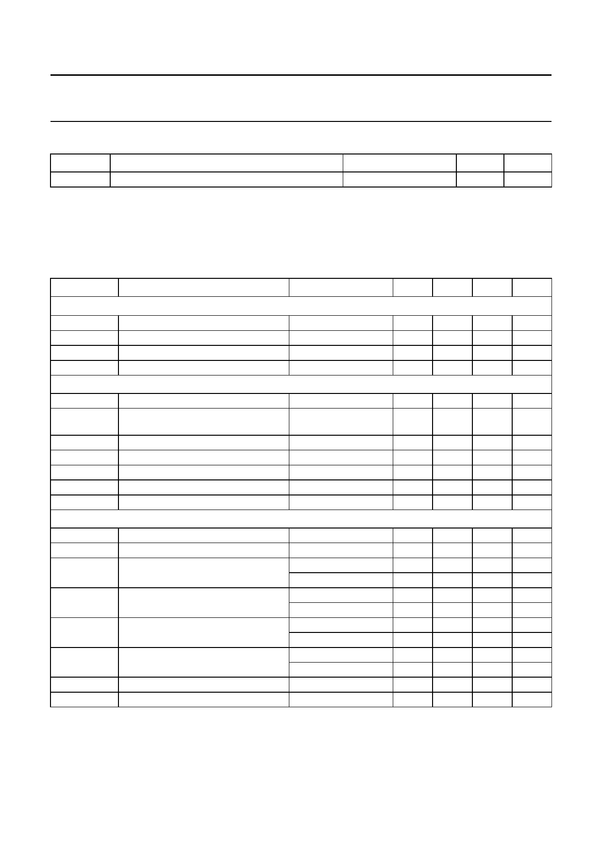
THERMAL CHARACTERISTICS
SYMBOL
PARAMETER
CONDITIONS
VALUE UNIT
Rth(j-mb)
thermal resistance from junction to mounting base note 1
4
K/W
Note
1. To minimize the thermal resistance from mounting base to heatsink [Rth(mb-h)] follow the recommended mounting
instruction: screw mounting preferred; torque = 40 Ncm; use heatsink compound; isolation plate increases Rth(mb-h).
CHARACTERISTICS
VP = 12 V; Tamb = 25 °C; VFB = 40 V; voltages referenced to ground (pin GND); unless otherwise specified.
SYMBOL
PARAMETER
CONDITIONS
MIN. TYP. MAX. UNIT
DC supplies (pins VP and VFB)
VP
VFB
Iq(FB)
Iq(P)
supply voltage
flyback supply voltage
quiescent flyback current
quiescent supply current
Input stage (pins INP, INN and FEEDB)
note 1
no load; no signal
Idefl = 0
8.2
−
VP + 6 −
−
2.5
−
80
25
V
60
V
4
mA
130 mA
Ii(dif)
Ii(dif)(offset)
IINP, IINN
Vclamp(INP)
Vclamp(INN)
IFEEDB
VFEEDB
differential input current
differential input offset current
[Ii(dif)(offset) = IINP − IINN]
single-ended input current
input clamp voltage on pin INP
input clamp voltage on pin INN
feedback current
feedback voltage
Output stages (pins OUTA and OUTB)
note 2
−
Idefl = 0; Rref = 3 kΩ; 0
Rm = 1 Ω
0
IINP = IINN = 0; note 3 2.7
IINP = IINN = 0; note 3 2.7
−
1
±500 ±600 µA
−
±20 µA
±300
3.0
3.0
±250
−
±600 µA
3.3
V
3.3
V
±300 µA
VP − 1 V
Idefl(p-p)
deflection current (peak-to-peak value)
0.6
−
IOUTA, IOUTB output current
±0.3 −
Vsat(OUTA-GND) saturation voltage pin OUTA to
pin GND
IOUTA = 0.7 A
−
1.1
IOUTA = 1.25 A; note 4 −
1.6
Vsat(VP-OUTA) saturation voltage pin VP to pin OUTA IOUTA = 0.7 A
−
2.1
IOUTA = 1.25 A; note 4 −
2.8
Vsat(OUTB-GND) saturation voltage pin OUTB to
pin GND
IOUTB = 0.7 A
−
1.1
IOUTB = 1.25 A; note 4 −
1.6
Vsat(VP-OUTB) saturation voltage pin VP to pin OUTB IOUTB = 0.7 A
−
1.0
IOUTB = 1.25 A; note 4 −
1.6
LE
linearity error
Idefl = ±0.7 A; note 5 −
−
VOUTA, VOUTB DC output voltage
Ii(dif) = 0; closed loop 5.1
5.7
2.5
A
±1.25 A
1.3
V
1.8
V
2.7
V
3.4
V
1.3
V
1.8
V
1.4
V
2.0
V
2
%
6.3
V
2003 Feb 05
6
Share Link: 