TEA1066T 데이터 시트보기 (PDF) - Philips Electronics
부품명
상세내역
제조사
TEA1066T Datasheet PDF : 24 Pages
| |||
Philips Semiconductors
Versatile telephone transmission circuit
with dialler interface
Product specification
TEA1066T
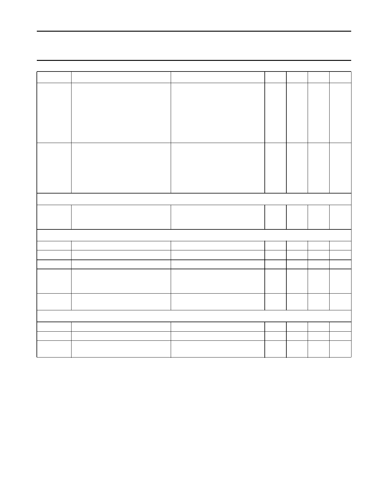
SYMBOL
PARAMETER
CONDITIONS
Vo(rms)
output voltage (RMS value)
Vno(rms)
noise output voltage (RMS value)
Gain adjustment GAR (pin 6)
sine-wave drive; Iline = 15 mA;
Ip = 0 mA; THD = 2%;
R4 = 100 kΩ
single-ended; RL = 150 Ω
single-ended; RL = 450 Ω
differential; CL = 47 nF;
Rseries = 100 Ω; f = 3400 Hz
Iline = 15 mA; R4 = 100 kΩ;
pin 13 (IR) open;
psophometrically weighted
(P53 curve)
single-ended; RL = 300 Ω
differential; RL = 600 Ω
∆Gv
gain variation with R4 connected
between pin 6 and pin 5 receiving
amplifier
MUTE input (pin 16)
VIH
VIL
IMUTE
∆Gv
Gv
HIGH level input voltage
LOW level input voltage
input current
voltage gain reduction between
MICL+ (pin 9) and MICL− (pin 7) to
LN (pin 1)
voltage gain from DTMF to QR+ or
QR−
MUTE = HIGH
MUTE = HIGH; R4 = 100 kΩ;
single-ended; RL = 300 Ω
Power-down input PD (pin 14)
VIH
HIGH level input voltage
VIL
LOW level input voltage
IPD
input current in power-down
condition
MIN. TYP. MAX. UNIT
0.30 0.38 −
V
0.40 0.52 −
V
0.80 1.0 −
V
−
50 −
µV
−
100 −
µV
−8 −
+8 dB
1.50 −
−
−
−
5
−
70
VCC V
0.3 V
10 µA
−
dB
−21 −19 −17 dB
1.5 −
−
−
−
5
VCC V
0.3 V
10 µA
1996 Apr 04
11
Share Link: 