TEA1733LT 데이터 시트보기 (PDF) - NXP Semiconductors.
부품명
상세내역
제조사
TEA1733LT Datasheet PDF : 20 Pages
| |||
NXP Semiconductors
TEA1733T; TEA1733LT
GreenChip III SMPS control IC
7. Functional description
7.1 General control
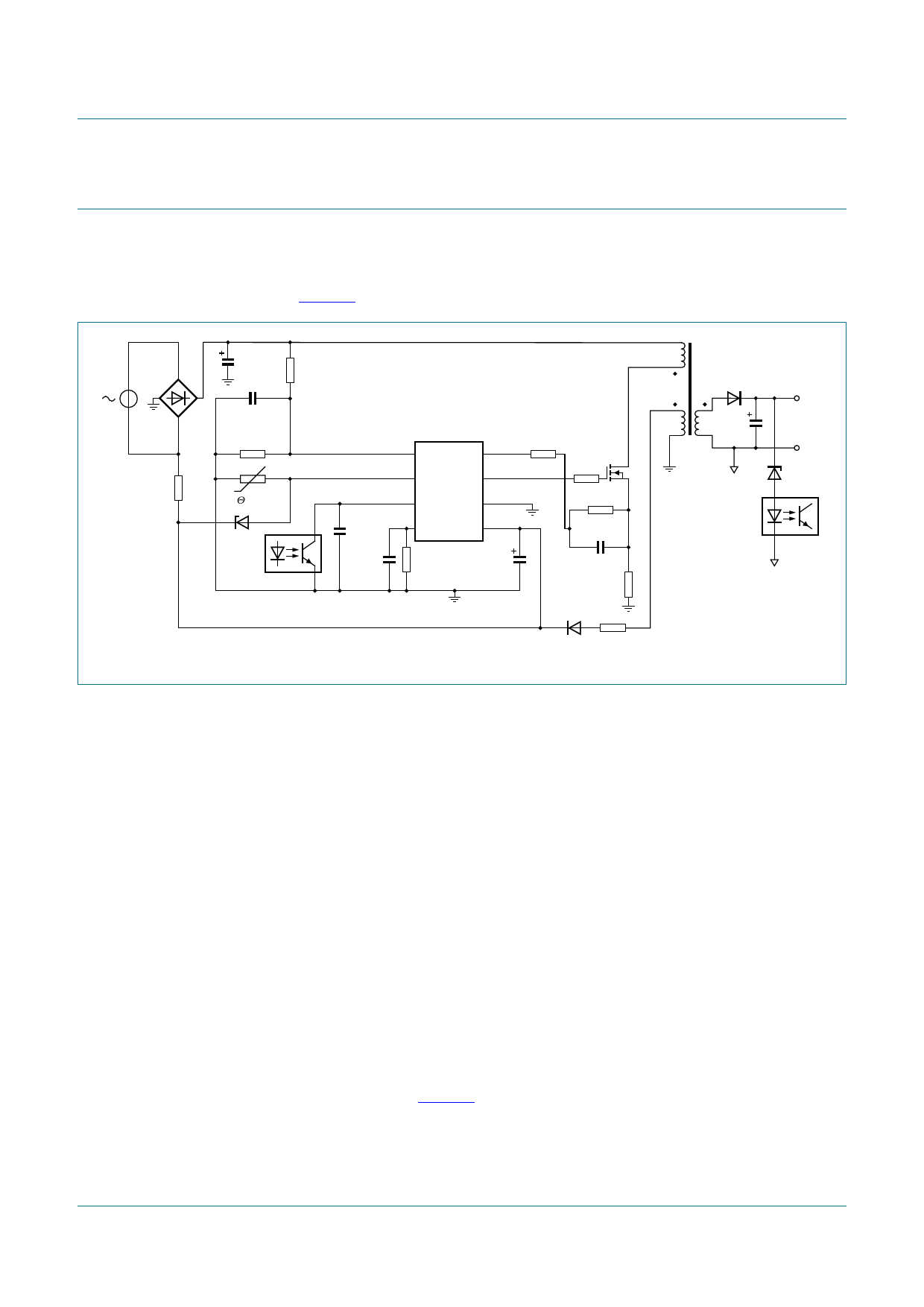
The TEA1733(L) contains a flyback circuit controller, a typical configuration of which is
shown in Figure 3.
C1
R1
C2
R2
R3
R4
Θ
Z1
TEA1733T
VINSENSE 5
PROTECT 6
4 ISENSE
R5
3 DRIVER
CTRL 7
OPTIMER
8
C3
2 GND
1 VCC
C4
R8
C5
S1
R10
R6
C6
R9
Fig 3. Typical configuration
R7
014aaa928
7.2 Start-up and UnderVoltage LockOut (UVLO)
Initially, the capacitor on the VCC pin is charged from the high voltage mains via resistor
R3.
If VCC is lower than Vstartup, the IC current consumption is low (typically 10 μA). When VCC
reaches Vstartup, the IC first waits for the VINSENSE pin to reach the Vstart(VINSENSE)
voltage and PROTECT pin to reach the Vdet(PROTECT)(L) voltage. When both levels are
reached, the IC charges the ISENSE pin to the Vstart(soft) level and starts switching. In a
typical application the supply voltage is taken over by the auxiliary winding of the
transformer.
If a protection is triggered the controller stops switching. Depending on the protection
triggered and IC version (TEA1733T or TEA1733LT), the protection causes a restart or
latches the converter to an off-state.
A restart caused by a protection rapidly charges the OPTIMER pin to 4.5 V (typical). The
TEA1733(L) enters Power-down mode until the OPTIMER pin discharges down to 1.2 V
(typical). In Power-down mode, the IC consumes a very low supply current (10 μA typical)
and the VCC pin is clamped at 22 V (typical) by an internal clamp circuit. When the
voltage on pin OPTIMER drops below 1.2 V (typical) and the VCC pin voltage is above the
VCC start-up voltage (See Figure 4), the IC restarts.
When a latched protection is triggered, the TEA1733(L) immediately enters Power-down
mode. The VCC pin is clamped to a voltage just above the latch protection reset voltage
(Vrst(latch) + 1 V).
TEA1733T_TEA1733LT_2
Product data sheet
All information provided in this document is subject to legal disclaimers.
Rev. 02 — 26 March 2010
© NXP B.V. 2010. All rights reserved.
5 of 20
Share Link: 