HT23C512 데이터 시트보기 (PDF) - Holtek Semiconductor
부품명
상세내역
제조사
HT23C512 Datasheet PDF : 12 Pages
| |||
A.C. test conditions
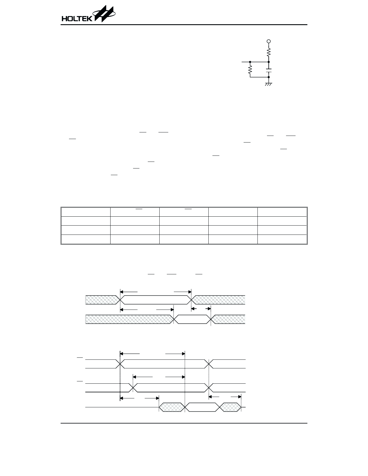
Output load: see figure right
Input rise and fall time: 10ns
Input pulse levels: 0.4V to 2.4V
Input and output timing reference levels:
0.8V and 2.0V (VCC=5V), 1.5V (VCC=3V)
O u tp u t
7759
HT23C512
V CC
12509
100p.*
* In c lu d in g s c o p e a n d jig
Output load circuit
Functional Description
The HT23C512 has two modes, namely data read mode
and standby mode, controlled by CE/CE/OE1/OE1 and
OE/OE/NC inputs.
· Standby mode
The HT23C512 has lower current consumption, con-
trolled by the chip enable input (CE/CE). When a
low/high level is applied to the CE/CE input regardless of
the output enable (OE/OE/NC) states, the chip will enter
the standby mode.
· Data read mode
When both the chip enable (CE/CE/OE1/OE1) and
the output enable (OE/OE/NC) are active, the chip is
in data read mode. Otherwise, active CE/CE and inac-
tive OE/OE/NC result in deselect mode. The output
will remain in Hi-Z state.
Operation Truth Table
Mode
CE/CE
Read
H/L
Deselect
H/L
Standby
L/H
Note: H=VIH, L=VIL, X=VIH or VIL
OE/OE
H/L
L/H
X
A0~A15
Valid
X
X
Timing Diagrams
· Propagation delay due to address (CE/CE/OE1/OE1 and OE/OE are active)
A d d re s s
D out
tC Y C
V a lid
tA A
tO H
V a lid
D0~D7
Data Out
High Z
High Z
· Propagation delay due to chip enable and output enable (address valid)
CE
CE
CE
OE
D out
tA C E
tA O E
tO E
tO D
V a lid
Rev. 1.10
4
August 30, 2002
Share Link: 