ADV7128KR50 데이터 시트보기 (PDF) - Analog Devices
부품명
상세내역
제조사
ADV7128KR50 Datasheet PDF : 8 Pages
| |||
ADV7128
It is important to note that while the ADV7128 contains cir-
cuitry to reject power supply noise, this rejection decreases with
frequency. If a high frequency switching power supply is used,
the designer should pay close attention to reducing power sup-
ply noise. A dc power supply filter (Murata BNX002) will pro-
vide EMI suppression between the switching power supply and
the main PCB. Alternatively, consideration could be given to
using a three terminal voltage regulator.
Digital Signal Interconnect
The digital signal lines to the ADV7128 should be isolated as
much as possible from the analog outputs and other analog cir-
cuitry. Digital signal lines should not overlay the analog power
plane.
Due to the high clock rates used, long clock lines to the
ADV7128 should be avoided so as to minimize noise pickup.
Any active pull-up termination resistors for the digital inputs
should be connected to the regular PCB power plane (VCC), and
not the analog power plane.
Analog Signal Interconnect
The ADV7128 should be located as close as possible to the out-
put connectors thus minimizing noise pickup and reflections
due to impedance mismatch.
The video output signals should overlay the ground plane, and
not the analog power plane, thereby maximizing the high fre-
quency power supply rejection.
For optimum performance, the analog outputs should each have
a source termination resistance to ground of 75 Ω (doubly ter-
minated 75 Ω configuration). This termination resistance should
be as close as possible to the ADV7128 so as to minimize
reflections.
Additional information on PCB design is available in an applica-
tion note entitled “Design and Layout of a Video Graphics Sys-
tem for Reduced EMI.” This application note is available from
Analog Devices, publication number E1309-15-10/89.
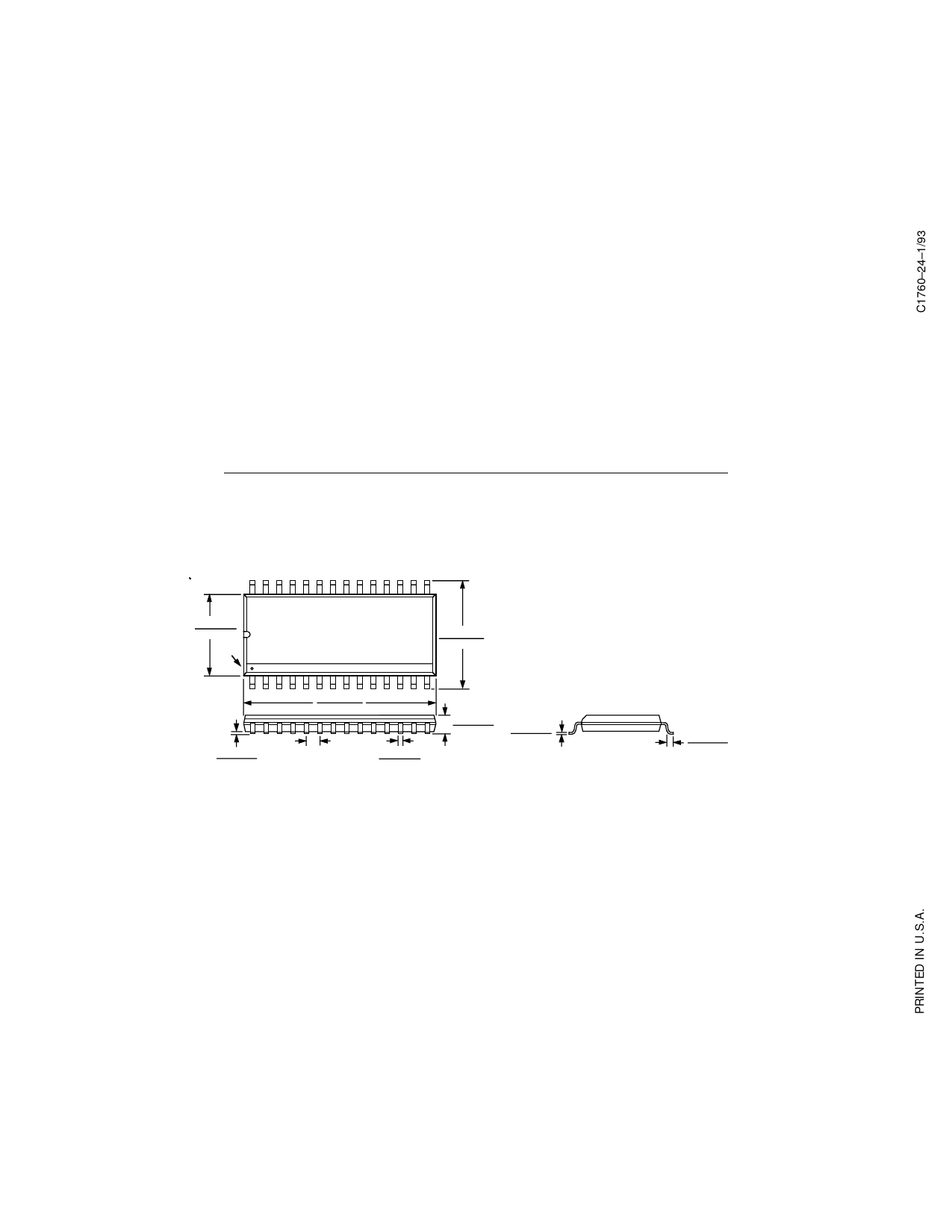
OUTLINE DIMENSIONS
Dimensions shown in inches and (mm).
SOIC (R-28)
28
0.299 (7.60)
0.291 (7.40)
PIN 1
1
15
0.419 (10.65)
0.394 (10.00)
14
0.011 (0.30)
0.004 (0.10)
0.712 (18.10)
0.697 (17.70)
0.050 (1.27)
BSC
0.019 (0.49)
0.014 (0.35)
0.104 (2.65)
0.093 (2.35)
0.012 (0.32)
0.009 (0.23)
0.05 (1.27)
0.016 (0.40)
–8–
REV. 0
Share Link: 