CDP68HC68W1 데이터 시트보기 (PDF) - Intersil
부품명
상세내역
제조사
CDP68HC68W1 Datasheet PDF : 9 Pages
| |||
CDP68HC68W1
chip. Deselection will transfer 16 bits of data from the shift
register into the frequency register and PW register. The
updated frequency and PW information will appear at the
PWM output pin only after the end of the previous total
output period.
Altering the Control Word: Changing the clock divider
and/or power control bit in the CDPHC68W1 control register
requires full 24-bit programming, as described under Power
Up Initialization.
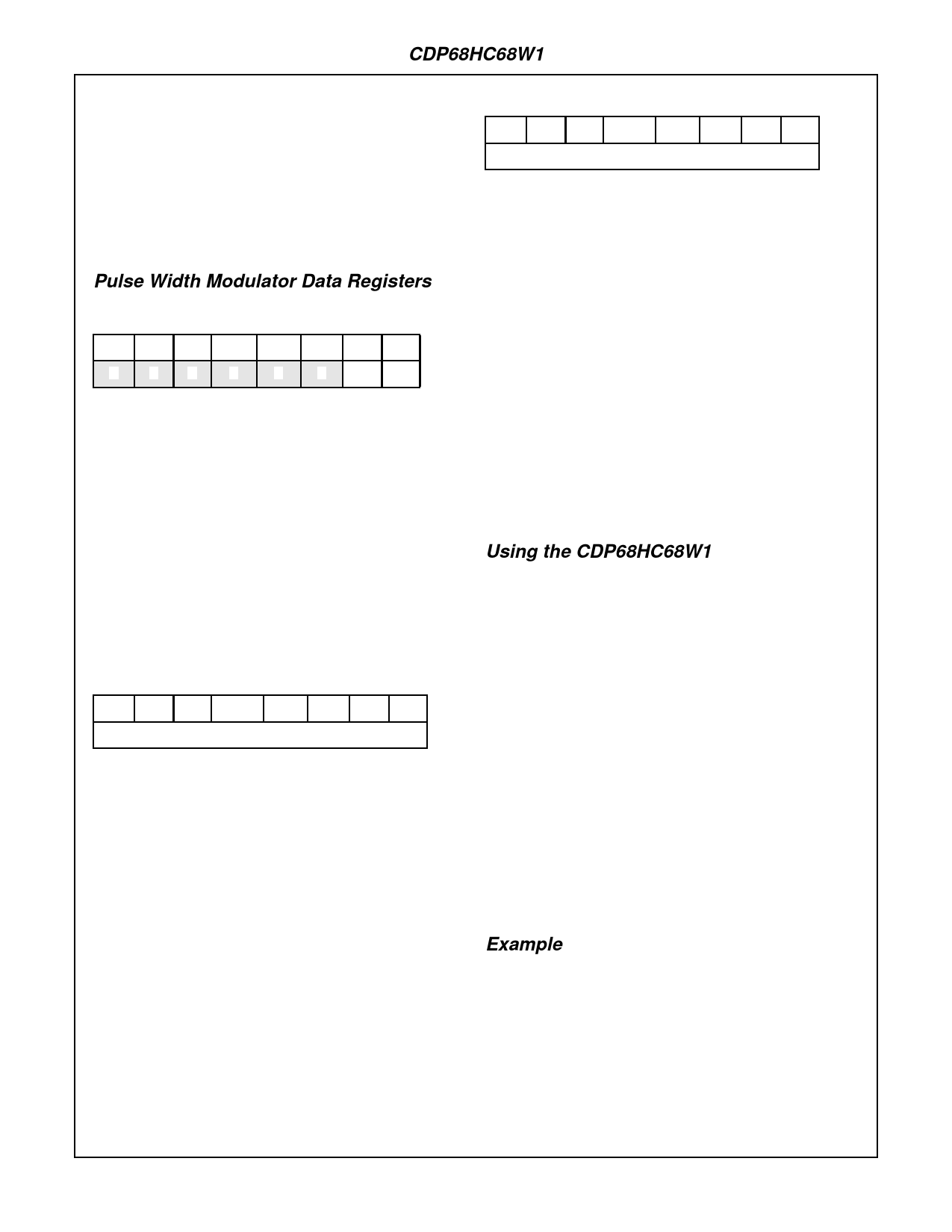
Pulse Width Modulator Data Registers
Byte 1: Control Register
7
65
4
3
2
1
0
0
00
0
0
0 PC CD
B7-B2
B2, PC
B0, CD
Unused; “don’t care”.
Power Control Bit. If this bit is a “0”, the chip will
remain in the active state. If the bit is set to a “1”,
internal clocking and the voltage comparator
(VT) circuit and voltage reference will be
disabled. Thus the chip will enter a low current
drain mode. The chip may only reenter the
active mode by clearing this bit and clocking in a
full 24 bits of information.
Clock Divider Bit. If this bit is a “0”, the chip will
set internal clocking (CLK) at a divide-by-one
rate with respect to the (CLK). If this bit is set to
“1”, the internal clocking will be set to divide-by-2
state.
Byte 2: Frequency Data Register
7
6
5
4
3
2
10
PWM Frequency Register
B7-B0
This register contains the value that will deter-
mine the output frequency or total period by:
Byte 3: Pulse Width Data Register
7
6
5
4
3
2
10
Pulse Width Data Register
B7-B0
This register contains the value that will
determine the pulse width or duty cycle (high
duration) of the output PWM waveform.
PW = (N+1) (CD+1)
PW = Pulse width out as measured in number of
input CLK periods.
CD = Value of clock divider bit in control register.
N = Value in PW register.
For a case of n (binary value in PW register)
equal to 3 and CD (clock divider) = 0 (divide-by-
1), the output will be 4 input clock periods of a
high level followed by the remaining clocks of the
total period which will be a low level.
Assuming the frequency register contains a
value of 5, the resultant PWM output would be
high for 4 CLK periods, low for 2.
Using the CDP68HC68W1
Programming the CDP68HC68W1
1. Select chip
2. Write to control register
3. Write to frequency register
4. Write to pulse width register
5. Deselect chip
NEXT - TO then alter the pulse width
1. Select chip
2. Write to pulse width register*
3. Deselect chip
FOUT = (---N------+-----1---F)---(-I-C-N----D------+-----1----)
FOUT = resultant PWM output frequency
FIN = the frequency of input CLK
n = value in frequency register
CD = value of clock divider bit in control register.
OR - To then alter the frequency (and possibly PW):
1. Select chip
2. Write to frequency register*
3. Write to pulse width register*
4. Deselect chip
NOTE: All writes use 8-bit words
Example
For a case of n (binary value in frequency
register) equal to 5, CD (clock divider) = 0
(divide-by-1), the PWM output will be a fre-
quency 1/6 that of the input clock (CLK). Like-
wise, the output clock period will be equal to 6
input CLK periods.
when CD = 0,
When CD=0, frequency register = 4, pulse width register = 1;
output = high for 2 input CLK periods, low for 3;
1. Select chip
2. Then write (most significant bit first) to the control, the fre-
quency, and pulse width registers (control = 00, frequency =
04, PW = 1)
6
Share Link: 