CDP68HC68T1 데이터 시트보기 (PDF) - Intersil
부품명
상세내역
제조사
CDP68HC68T1 Datasheet PDF : 23 Pages
| |||
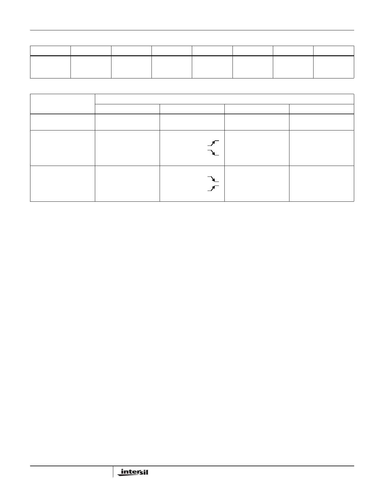
STATUS REGISTER (Read Only) - Address 30H
D7
D6
D5
0
WATCHDOG
TEST
MODE
MODE
CE
DISABLE
L
RESET
WRITE
H
CDP68HC68T1
D4
FIRST
TIME
UP
D3
INTERRUPT
TRUE
D2
POWER
SENSE
INTERRUPT
D1
ALARM
INTERRUPT
D0
CLOCK
INTERRUPT
TRUTH TABLE
SIGNAL
SCK (Note 9)
MOSI
INPUT DISABLED
INPUT DISABLED
MISO
HIGH Z
CPOL = 1
DATA BIT LATCH
HIGH Z
READ
CPOL = 0
H
CPOL = 1
X
NEXT DATA BIT
SHIFTED OUT
(Note 10)
CPOL = 0
NOTES:
9. When interfacing to CDP68HC05 microcontrollers, serial clock phase bit, CPHA, must be set = 1 in the microcomputer’s Control Register.
10. MISO remains at a high Z until 8-bits of data are ready to be shifted out during a READ. It remains at a high Z during the entire WRITE cycle.
Watchdog
If this bit is set high, the watchdog circuit has detected a
CPU failure.
Test Mode
When this bit is set high, the device is in the TEST MODE.
First-time Up
Power-on reset sets this bit high. This signifies that data in
the RAM and Clock is not valid and should be initialized.
Interrupt True
A high in this bit signifies that one of the three interrupts
(Power Sense, Alarm, and Clock) is valid.
Power-sense Interrupt
This bit set high signifies that the power-sense circuit has
generated an interrupt.
Alarm Interrupt
When the seconds, minutes and hours time and alarm
counter are equal, this bit will be set high. Status Register
must be read before loading Interrupt Control Register for
valid alarm indication after alarm activates.
Clock Interrupt
A periodic interrupt will set this bit high.
All bits are reset by a power-on reset except the “FIRST-
TIME UP” which is set. All bits except the power-sense bit
are reset after a read of this register.
Pin Signal Description
SCK (Serial Clock Input) (Note 11)
This input causes serial data to be latched from the MOSI
input and shifted out on the MISO output.
MOSI (Master Out/Slave In) (Note 11)
Data bytes are shifted in at this pin, most significant bit
(MSB) first.
MISO (Master In/Slave Out)
Data bytes are shifted out at this pin, most significant bit
(MSB) first.
CE (Chip Enable) (Note 12)
A positive chip-enable input. A low level at this input holds
the serial interface logic in a reset state, and disables the
output driver at the MISO pin.
NOTES:
11. These inputs will retain their previous state if the line driving them
goes into a High-Z state.
12. The CE input has as internal pull-down device, if the input is in a
low state before going to High Z, the input can be left in a High Z.
13
FN1547.8
October 29, 2007
Share Link: 