TPC8120 데이터 시트보기 (PDF) - Toshiba
부품명
상세내역
제조사
TPC8120 Datasheet PDF : 7 Pages
| |||
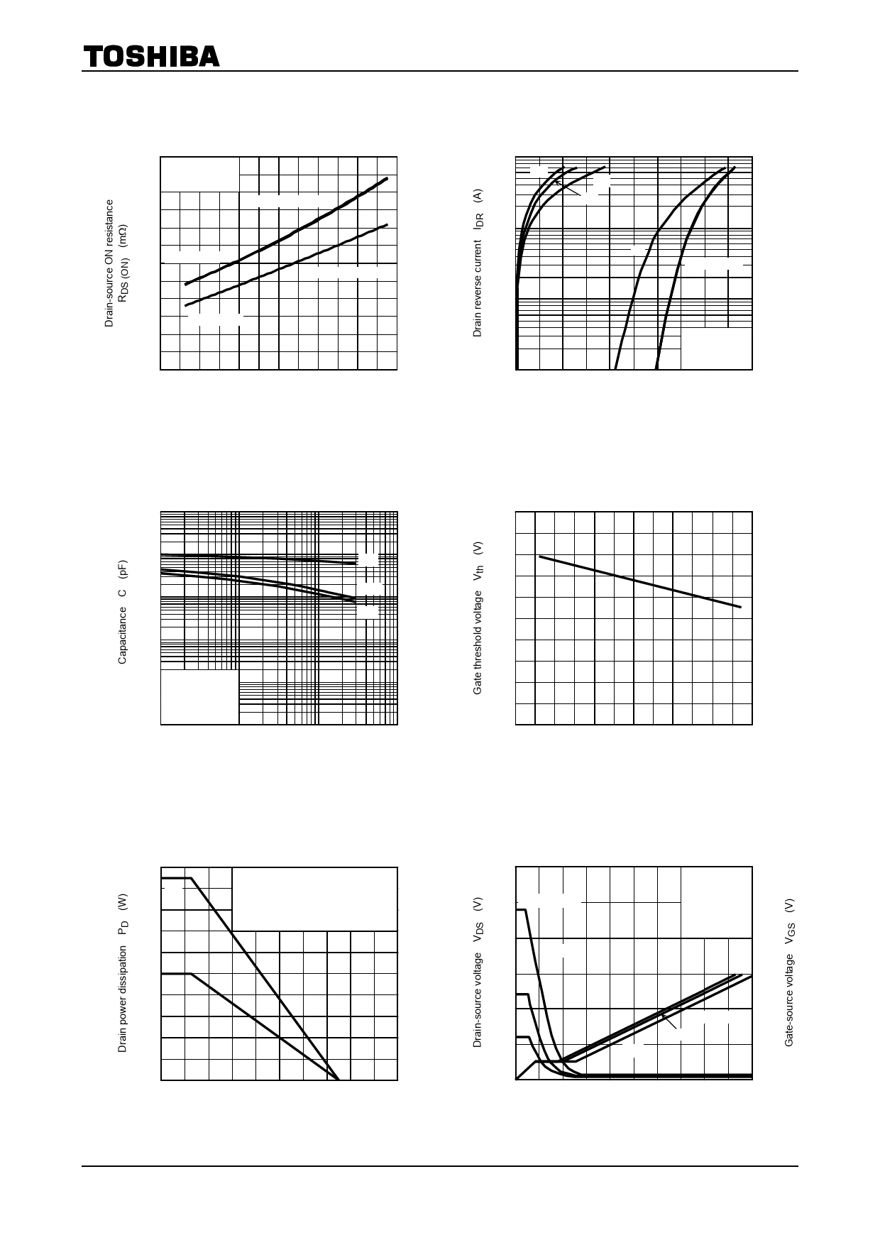
RDS (ON) – Ta
6
Common source
Pulse test
5
ID = −4.5, −9, −18 A
4
3 VGS = −4.5 V
2
VGS = −10 V
1
ID = −4.5, −9, −18 A
0
−80
−40
0
40
80
120
160
Ambient temperature Ta (°C)
TPC8120
−100
−10
−10
−1
IDR – VDS
−3
−4.5
−1
VGS = 0,1 V
−0.1
0
Common source
Ta = 25°C
Pulse test
0.2
0.4
0.6
0.8
1
Drain-source voltage VDS (V)
100000
Capacitance – VDS
10000
1000
100
Ciss
Coss
Crss
10 Common source
VGS = 0 V
f = 1 MHz
Ta = 25°C
1
−0.1
−1
−10
Drain-source voltage VDS (V)
−100
Vth – Ta
−2
−1.6
−1.2
−0.8
Common source
−0.4 VDS = −10 V
ID = −1 mA
Pulse test
0
−80
−40
0
40
80
120
160
Ambient temperature Ta (°C)
2
(1)
1.6
1.2
(2)
0.8
PD – Ta
(1) Device mounted on a glass-epoxy board
(a) (Note 2a)
(2) Device mounted on a glass-epoxy board
(b) (Note 2b)
t = 10 s
0.4
0
0
40
80
120
160
200
Ambient temperature Ta (°C)
Dynamic input/output characteristics
−30
−30
VDD = −24V
Common source
ID = −18 A
Ta = 25°C
Pulse test
−20
−20
VDS
−12
−10
−6
0
0
−6
VGS
−10
VDD = −24V
−12
50
100
150
200
Total gate charge Qg (nC)
0
250
5
2009-07-27
Share Link: 