TPS830 데이터 시트보기 (PDF) - Toshiba
부품명
상세내역
제조사
TPS830 Datasheet PDF : 6 Pages
| |||
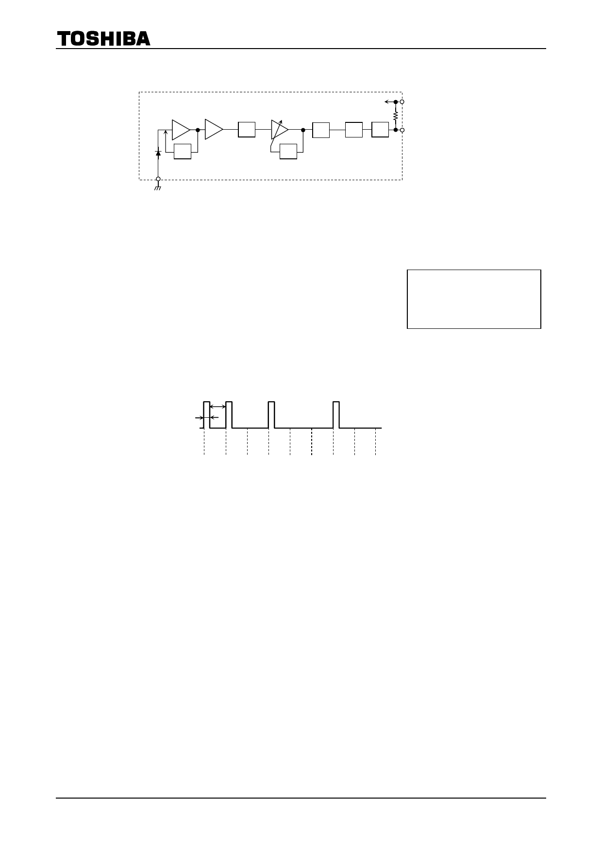
Circuit Block Diagram
I-V
Preamp.
BPF
AGC
Envelope
Output
PD
LPF
Average
Slicer
3. VCC
1. VO
2. GND
TPS830(F)
Bit Pattern Designing Example (reference)
• Example of code signal = 11010010
Sequence of LED signals = 1 must be avoided. If LED signals of 1
sequence, TPS830(F) may not receive LED signals properly. After an LED
signal of 1, 0 must be sent (55μ or longer interval necessary).
Please take this into account when designing a bit pattern.
The following shows the bit pattern t example that is converted at first
code signals to LED signals as shown on the right diagram.
<Conversion example>
Code signal LED signal
0
→
00
1
→
10
<Pattern example>
LED signals
1 0 10 00 1 0 0 0 0 0 100 0
62μs
26μs
Code signals 1 1 0 1 0 0 1 0
Precautions
1. To stabilize the power line, insert a bypass capacitor of up to 0.01μF between VCC and GND, close to the
device.
2. At power−on the internal circuit takes about 100μs to stabilize. During this period the output signal is unstable
and may change.
3. To avoid unnecessary oscillation, insert a bypass capacitor of 1000pF between VCC and GND.
4. When using the device, please take the device’s characteristics, the operating environment and the
characteristics of pairing LED device into considerations.
5. Soldering temperature: ≦ 260°C, soldering time : ≦ 5s (Soldering must be performed under the 2mm from
the body of the device.)
6. When forming the leads, bend each lead under the 2mm from the body of the device. Soldering must be
performed after the leads have been formed.
4
2007-10-01
Share Link: 